The capital-equipment and materials layer that enables all semiconductor's manufacturing — its structure, economics, leaders, and strategic risks.
Executive summary
The semiconductor equipment and semiconductor materials industry supplies the capital tools and consumable inputs required to manufacture every integrated circuit produced worldwide. It sits at the apex of the chip supply chain: its customers are the chip designers/fablesses, foundries, integrated device manufacturers (IDMs), and outsourced assembly-and-test houses (OSAT) that together constitute the rest of the industry. Because no advanced chip can be fabricated without these tools and materials, the sector functions as the binding constraint on global computing capacity — a position that confers both unusual pricing power and acute strategic sensitivity.
Three characteristics define the sector’s investment profile. First, structural concentration: a handful of firms control the majority of each process step, and several occupy de facto monopolies. 2) Second, deep and durable barriers to entry: leading-edge tools embody decades of accumulated process physics and are co-developed with customers years ahead of production, making displacement rare. Third, geopolitical centrality: because controlling the means of production is the most effective lever for controlling who can manufacture advanced chips, the sector has become the principal instrument of export-control policy between the United States, its allies, and China.
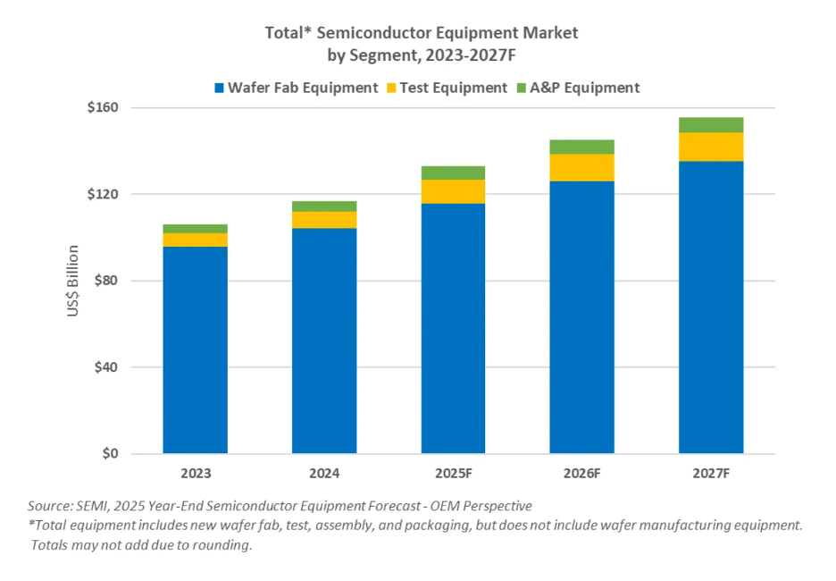
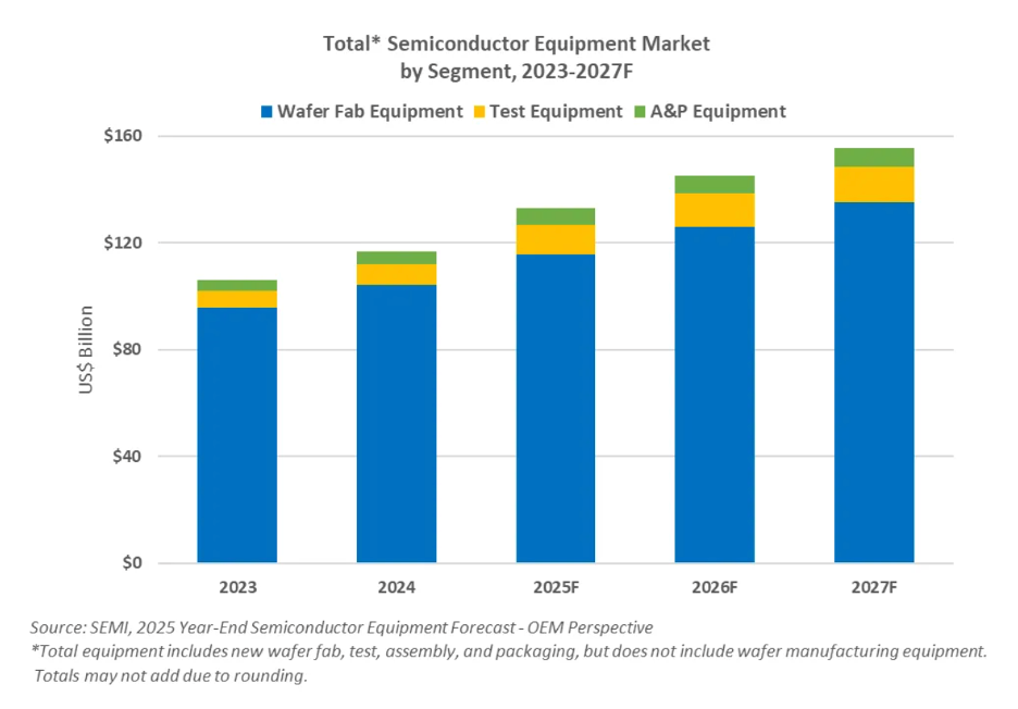
On the latest data, total semiconductor equipment sales reached a record $135 billion in 2025 and are forecast by SEMI to surpass $150 billion for the first time in 2027 (~$156 billion) (SEMI), while the separately-reported materials market set a record of $73.2 billion in 2025 (SEMI). The current cycle is distinguished less by unit volume than by complexity: artificial intelligence, high-bandwidth memory, and advanced packaging are reshaping where capital is deployed across the manufacturing flow.
1. Defining the sector and its strategic importance
For semiconductor equipments, a useful starting point is the economics of a modern fabrication plant (“fab”). A single leading-edge logic fab now requires a capital outlay on the order of $20–30 billion or more, of which the great majority — commonly 70–80% — is spent on process equipment rather than the building itself, based on our channel check and industry analysis. The equipment industry therefore captures the largest share of every wave of fab investment, and its revenues are a direct function of the capital-expenditure decisions of a small number of very large manufacturers (for example, TSMC, Samsung, Intel, and the memory producers).
The materials industry operates on a different rhythm. Where equipment is a periodic capital purchase, materials — silicon wafers, photoresist, process gases, substrates — are consumed continuously as long as a fab is running. This gives the materials business steadier, utilization-linked revenue that is far less volatile than equipment demand, an important distinction for portfolio construction.
Taken together, the sector is best understood not as a supplier of components but as the owner of the enabling technology for the entire digital economy. Its products are the precondition for every downstream activity, which is why a relatively modest revenue base (roughly $200 billion across equipment and materials combined in 2025, according to SEMI) commands disproportionate strategic and financial attention.
2. Position in the value chain
The chip moves through a sequential value chain, with equipment and materials feeding in from upstream. Crucially, equipments & materials supply both ends of manufacturing — the front-end fabs that build circuits on the wafer, and the back-end houses that package and test finished devices. The equipment vendor is always upstream of whoever operates the tool.
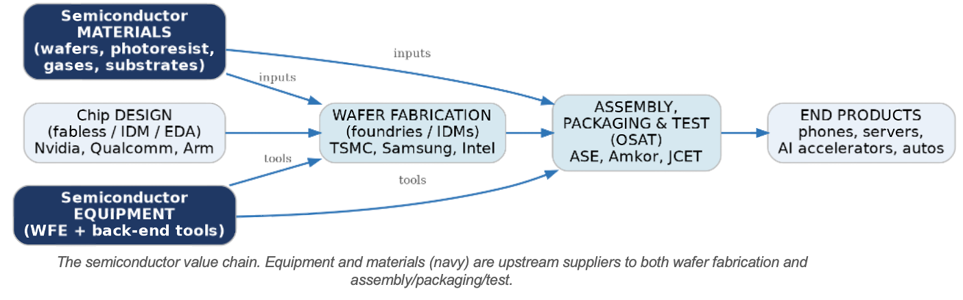
This distinction resolves a common point of confusion. “Assembly, packaging, and test” denotes both a service (performed downstream by OSAT firms such as ASE and Amkor) and the equipment used to perform it (supplied upstream by tool vendors). The back-end equipment is upstream of back-end manufacturing; the naming overlaps, but the economic roles do not.
3. How chips are made — and where each tool fits
Understanding the sector requires understanding the manufacturing flow, because each major equipment category maps to a specific process step. Fabrication divides into a front-end phase (building the transistors and interconnect on the wafer) and a back-end phase (singulating, packaging, and testing the finished chips).
Front-end: a repeated build-up of layers
The front-end does not run once; it is a cyclical process repeated 50 to more than 100 times, once for each layer of the device. A simplified cycle proceeds as follows:
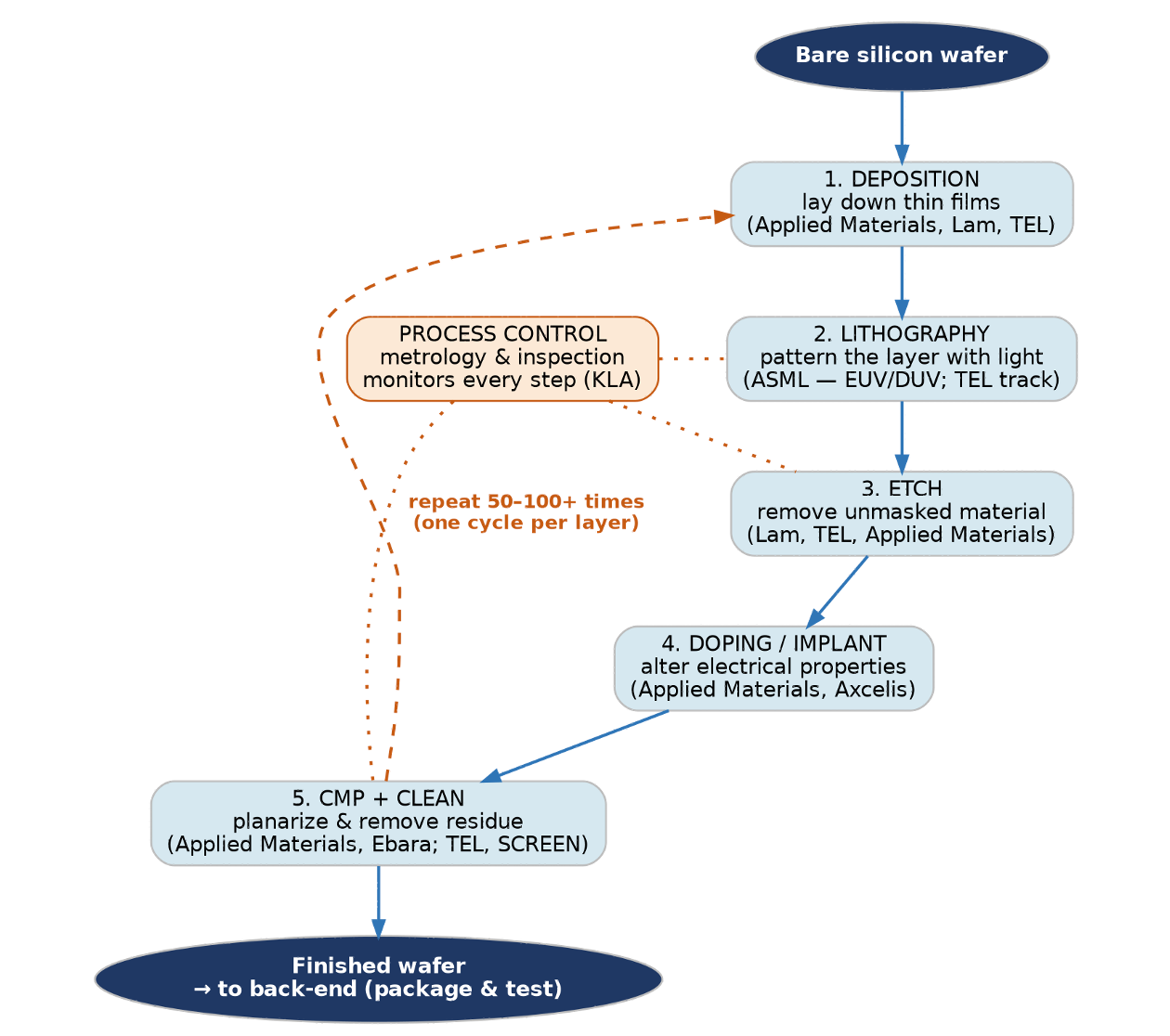
Each pass deposits material, patterns it with light, and etches away what is not needed, with doping, planarization, and cleaning interspersed. Because the cycle repeats so many times, even small per-step improvements in yield or throughput compound enormously — which is why customers are reluctant to switch qualified tools and why incumbents enjoy such durable positions. As devices migrate to advanced architectures (FinFET and now gate-all-around transistors, plus 3D memory stacking), the number of deposition and etch steps has risen sharply, increasing the equipment intensity of each wafer and benefiting the deposition/etch leaders in particular.
Back-end: from wafer to packaged, tested chip
Once the wafer is complete, the back-end dices it into individual dies, attaches and connects them within a package, and tests the result. Historically a lower-value, slower-growing segment, the back-end has been transformed by advanced packaging, which increasingly uses wafer-level, fab-style processes and so blurs the traditional front-end/back-end boundary.
4. Market size and segmentation
We summarize semiconductor equipment and materials in two separate SEMI data sets. The equipment figures come from SEMI’s Year-End Total Semiconductor Equipment Forecast; the materials figures come from SEMI’s annual Materials Market report. The two markets differ in size, segmentation, and cyclicality, so combining them obscures more than it reveals.
4.1 The equipment market
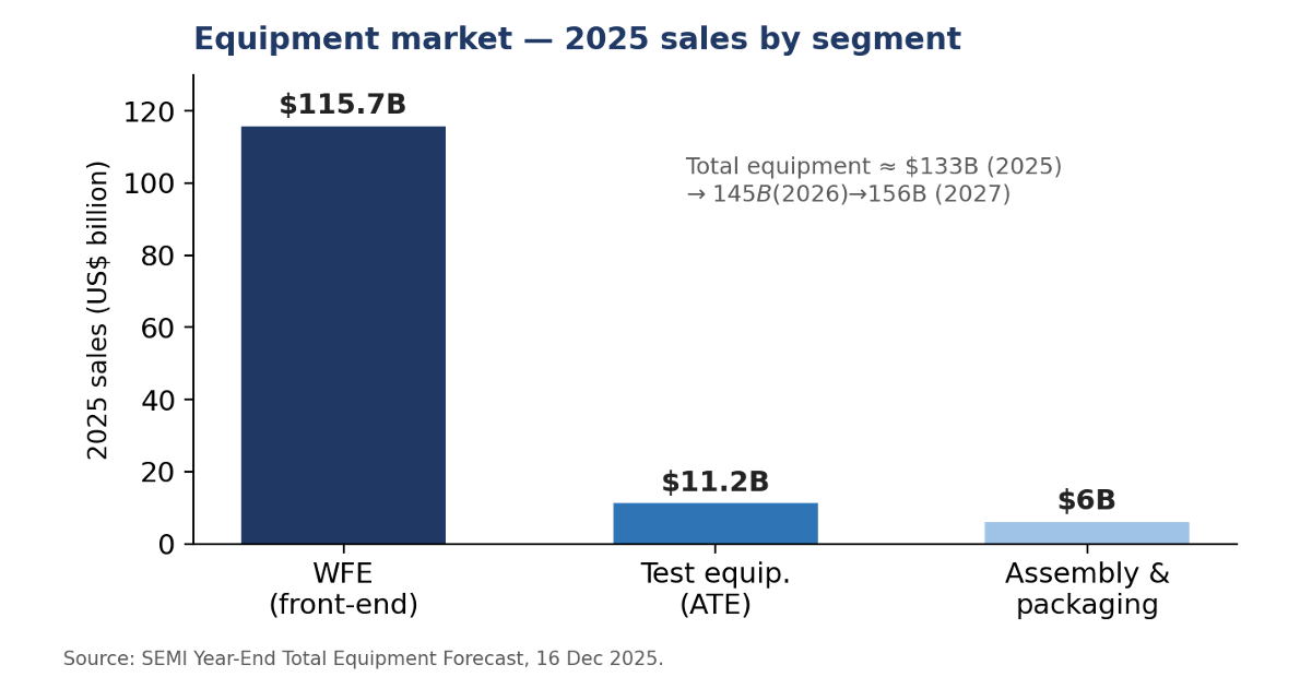
Per SEMI’s Year-End Total Equipment Forecast (16 December 2025), total semiconductor manufacturing equipment sales reached a record $133 billion in 2025 (+13.7% year-on-year), and are projected to grow to $145 billion in 2026 and $156 billion in 2027 — surpassing $150 billion for the first time. Wafer fab equipment (WFE) dominates, while the back-end (test and packaging) has rebounded sharply off a smaller base.
|
Equipment
segment |
2025 sales |
2025 growth |
Trajectory
to 2027 |
|
WFE (front-end) |
$115.7 bn |
+11.0% (from $104 bn in
2024) |
→ $135.2 bn by 2027
(advanced logic, DRAM/HBM) |
|
Test equipment (ATE) |
$11.2 bn |
+48.1% |
+12.0% 2026, +7.1% 2027 (AI/HBM test complexity) |
|
Assembly & packaging |
$6.0 bn |
+19.6% |
+9.2% 2026, +6.9% 2027
(advanced packaging) |
|
Total equipment |
$133 bn |
+13.7% |
→ $145 bn 2026 → $156 bn 2027 |
Within WFE, foundry-and-logic applications alone accounted for roughly $66.6 billion in 2025 (+9.8%), reflecting resilient leading-edge spending. China, Taiwan, and Korea are expected to remain the top three equipment-buying regions through 2027.
4.2 The materials market
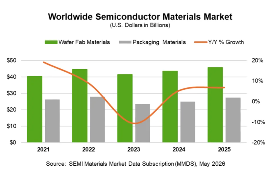
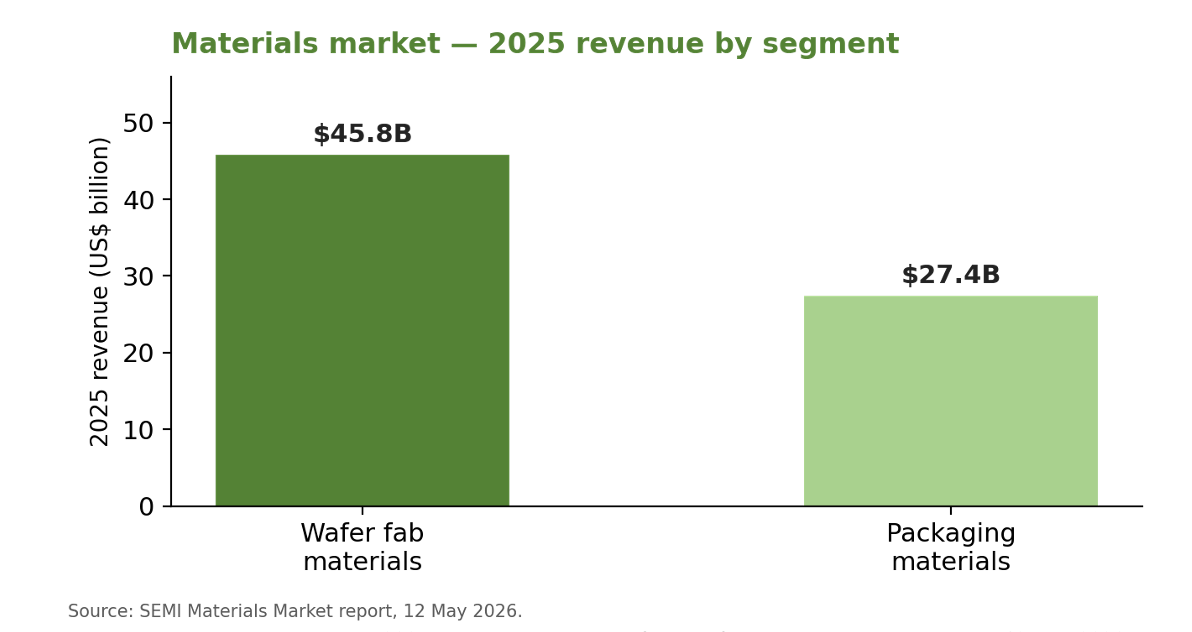
Per SEMI’s Materials Market report (12 May 2026) — a wholly separate release — global semiconductor materials revenue reached a record $73.2 billion in 2025 (+6.8% year-on-year). Materials are consumables purchased continuously as fabs run, so this market is steadier and less cyclical than equipment. It divides into wafer fab materials (used in front-end fabrication) and packaging materials (used in back-end assembly).
|
Materials
segment |
2025 revenue |
2025 growth |
Representative
inputs |
|
Wafer fab materials |
$45.8 bn |
+5.4% |
Silicon wafers, photoresist,
gases, CMP slurries, masks |
|
Packaging materials |
$27.4 bn |
+9.3% |
Substrates, bonding wire, lead frames, encapsulants |
|
Total materials |
$73.2 bn |
+6.8% |
— |
Geographically, the materials data show where chips are actually built. Taiwan was the largest consumer for the 16th consecutive year (~$21.7 billion in 2025), followed by China (~$15.6 billion) and South Korea (~$11.2 billion). A related SEMI release (Feb 2026) noted that silicon wafer shipments rose 5.8% in 2025 to a record area, even as wafer revenue dipped slightly — a sign that AI-driven demand is concentrated in higher-value advanced wafers.
|
Top
materials consumers (2025) |
Revenue |
|
Taiwan (16th consecutive
year as #1) |
~$21.7 bn |
|
China |
~$15.6 bn |
|
South Korea |
~$11.2 bn |
5. Equipment segments and their leaders
The front-end equipment market is segmented by process step, with a clear leader (often a near-monopolist) in each:
· Lithography — the highest-value and most concentrated step, patterning circuits onto the wafer with light. ASML is the sole producer of extreme-ultraviolet (EUV) systems, which use 13.5-nanometer light to print the smallest features; its next-generation High-NA EUV tools cost in excess of $350 million each. ASML also leads advanced deep-ultraviolet (DUV) immersion lithography, with Canon and Nikon present at older nodes.
· Deposition — building up thin films via CVD, PVD, ALD, and epitaxy. Led by Applied Materials, Lam Research, and Tokyo Electron (TEL). Atomic-layer deposition in particular has grown with gate-all-around transistors and 3D memory.
· Etch — selectively removing material. Lam Research and Tokyo Electron lead, with Applied Materials present; high-aspect-ratio etch for 3D NAND and advanced logic is a key battleground.
· Process control (metrology & inspection) — measuring dimensions and detecting defects to protect yield. KLA holds a commanding position, and its importance rises as devices grow more complex; this segment also carries the highest margins in the industry.
· Other front-end steps — cleaning and surface preparation (TEL, SCREEN), ion implantation (Applied Materials, Axcelis), chemical-mechanical planarization (Applied Materials, Ebara), and thermal processing. Notably, TEL holds an estimated 88–90% share of the coater/developer (“track”) tools that pair with lithography.
Back-end equipment is more fragmented but faster-growing:
· Assembly & packaging tools — wire, die, flip-chip, and hybrid bonders; leaders include ASMPT, Kulicke & Soffa, and Besi. Hybrid bonding is the critical enabler of 3D stacking.
· Test equipment (ATE) — a duopoly of Teradyne and Advantest; Advantest in particular has benefited from the surge in testing intensity for AI accelerators and HBM.
6. Materials segments and their leaders
Materials feature their own deep moats: a contaminant measured in parts-per-billion can destroy a wafer, qualification cycles run for years, and switching costs are high.
• Silicon wafers — the substrate, led by Shin-Etsu and SUMCO of Japan, with GlobalWafers and Siltronic also major. Worldwide wafer shipments rebounded in 2025–26 on AI demand (SEMI).
• Photoresist and ancillaries — light-sensitive chemicals central to lithography. Japanese suppliers — Tokyo Ohka Kogyo (TOK), JSR, and Shin-Etsu — together hold more than half the global market, with leadership in EUV and ArF-immersion resists. This is among the most R&D-intensive material categories.
• Specialty gases and wet chemicals — Air Liquide, Linde, Merck, and others; consumption rises with process-step count.
• Photomasks, CMP slurries/pads, and sputtering targets — specialized consumables across the front-end flow.
• Packaging materials — substrates (notably ABF substrate), bonding wire (cost tied to gold prices), lead frames, and encapsulants. The fastest-growing materials sub-segment, driven by advanced packaging and the higher material intensity of multi-die AI chips; packaging materials grew 9.3% to $27.4 billion in 2025 (SEMI).
7. Competitive structure and company financials
The sector’s defining commercial feature is oligopoly with monopoly pockets. The five largest equipment suppliers — Applied Materials, ASML, Tokyo Electron, Lam Research, and KLA — together command an estimated 56–66% of the equipment market, and the leader in each individual step typically holds a far higher share still.
The financial signature of this structure is high and persistent margins, substantial recurring service revenue, strong returns on equity, and large capital returns. The latest full-year results illustrate the point:
|
Company |
Core
franchise |
FY2025
revenue |
Gross margin |
Net income |
|
ASML |
Lithography (sole EUV maker) |
€32.7 bn (~$35 bn) |
52.8% |
€9.6 bn |
|
Applied Materials |
Broadest front-end + services |
$28.4 bn |
48.7% |
~$7.0 bn |
|
Lam Research |
Etch & deposition +
services |
$18.4 bn |
48.7% |
$5.36 bn |
|
KLA |
Process control / inspection |
$12.2 bn |
~60.9% |
$4.06 bn |
Several financial themes emerge from these disclosures:
• Margin hierarchy reflects competitive intensity. KLA’s ~61% gross margin — well above the ~49–53% of the others — reflects its dominant, lightly-contested position in process control. ASML’s margins are buoyed by the EUV monopoly.
• Recurring service revenue is a stabilizer. Service (spares, upgrades, field options on the installed base) is roughly 23% of revenue at ASML, Applied Materials, and KLA, and a notably higher ~43% at Lam Research — a meaningful cushion against the equipment cycle.
• Returns and capital allocation are aggressive. All five majors generate returns on equity above 30%. ASML authorized a new buyback of up to €12 billion (through 2028); Applied Materials repurchased ~$4.9 billion of stock in fiscal 2025. These are cash-generative, capital-light franchises.
• Customer and geographic concentration is high. Applied Materials’ two largest customers represented roughly 19% and 15% of revenue in FY2025; Lam Research derived 34% of fiscal-2025 revenue from China. Concentration is both a source of scale economics and a risk.
Tokyo Electron, the largest Japanese supplier and the third/fourth-largest globally, rounds out the front-end “big five” with its track dominance and strong etch/deposition franchises; precise figures follow its own (April-ending) fiscal calendar.
8. Demand drivers: an AI- and complexity-led cycle
The present up-cycle is driven by architecture and complexity rather than unit volume. The principal drivers:
Artificial intelligence and high-performance computing. Training and serving large models requires vast quantities of leading-edge logic and high-bandwidth memory (HBM), pulling WFE for advanced nodes and for DRAM/HBM capacity. KLA’s management has explicitly tied its return to leading-edge growth to “expanding AI and high-performance computing investments.”
The end of easy transistor scaling and the rise of advanced packaging. As shrinking transistors becomes harder and costlier, performance increasingly comes from packaging — stacking and interconnecting multiple dies and memory. The advanced-packaging market was roughly $33–38 billion in 2024–25, growing at a double-digit CAGR, and by some estimates surpassed traditional packaging as a majority of total packaging value in 2025 (Yole). TSMC’s CoWoS platform is the marquee example: CoWoS wafer demand is forecast to rise roughly 40% year-over-year into 2026, driven overwhelmingly by Nvidia.
Memory as a strategic asset. HBM has converted DRAM from a boom-bust commodity into a constrained, high-value product, prompting elevated memory-equipment spending. This is the proximate cause of the upward revisions to WFE forecasts through 2027.
Because advanced packaging increasingly relies on wafer-level processes, front-end-style tools (deposition, etch, lithography) are migrating into the back-end, expanding the addressable market for the large front-end vendors and partly explaining their strategic push into packaging.
9. The dominant risk: geopolitics and export controls
Export controls now move the sector’s share prices. The governing logic is that controlling the tools is more effective than controlling the chips: a lithography system is a ~$200 million asset requiring years of vendor servicing, whereas a finished chip is a commodity that can be rerouted. The United States and its allies (the Netherlands and Japan, home to ASML, TEL, Nikon, Canon, SCREEN, and Advantest) have progressively restricted exports of advanced equipment to China.
The state of play as of mid-2026:
• EUV is fully denied to China. ASML’s EUV tools have never been sold there; no domestic alternative exists, and China’s SMEE remains far behind on indigenous lithography.
• DUV and servicing are the live battleground. SMIC and Hua Hong still use ASML’s DUV immersion tools, applying multipatterning to reach 7nm-class chips. Proposed US legislation (the MATCH Act) would tighten DUV and etch controls and press allies to align.
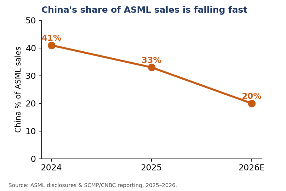
• Western vendors’ China exposure is falling sharply. China’s share of ASML sales declined from roughly 41% (2024) to 33% (2025), with guidance toward ~20% in 2026.
• China is accelerating self-sufficiency. Beijing has reportedly mandated at least 50% domestic equipment sourcing, with a 15th Five-Year-Plan target of ~80% self-sufficiency by 2030, a fully domestic 7nm equipment line, and stable 14nm production. Domestic suppliers (NAURA, AMEC, and SiCarrier-linked entities) are gaining share in mature-node and packaging tools.
The widely noted irony is that aggressive controls are accelerating China’s domestic investment, pushing the world toward two parallel supply chains. For investors this is double-edged: a near-term loss of a large market for Western vendors, and the longer-term emergence of subsidized domestic competitors at the low-to-mid end.
10. A framework for financial analysis
Several principles help in evaluating companies in the sector:
• Track the capex cycle through leading indicators. Equipment demand follows customer capital budgets; monitor the capex guidance of TSMC, Samsung, Intel, and the memory makers, plus fab-utilization rates and company backlog and bookings (ASML’s quarterly net bookings, which reached €13.2 billion in Q4 2025, are a closely watched signal).
• Use “WFE intensity” as a structural lens. Because each node transition adds deposition, etch, and patterning steps, WFE spending per wafer tends to rise structurally even when wafer volumes are flat — a secular tailwind beneath the cycle.
• Value the recurring base. Service and installed-base revenue is higher-margin and far steadier than tool sales; a larger service mix (e.g., Lam’s ~43%) warrants a more defensive valuation.
• Watch margin persistence and R&D intensity. Sustained high gross margins signal pricing power; sustained heavy R&D (ASML alone spent €4.7 billion in 2025) is the price of staying ahead — falling R&D is a warning, not a saving.
• Pair equipment with materials. Equipment offers torque to the capex cycle and the highest margins; materials offer steadier, utilization-linked revenue. Holding both balances cyclicality.
This document is an educational overview, not investment advice, and does not constitute a recommendation to buy or sell any security.
11. Key debates to watch
• Durability of the AI capex cycle — multi-year structural build-out versus eventual digestion and over-build.
• Who captures advanced packaging — foundries (TSMC), OSATs (ASE, Amkor), and equipment makers are all advancing; the economics of process and tool ownership are still being decided.
• Pace of China’s indigenization — mature nodes and packaging appear achievable; EUV and the most advanced steps remain a steep, multi-year climb.
• HBM/memory cyclicality — whether HBM stays supply-constrained or swings back to a glut is a key swing factor for memory-exposed equipment demand.
12. Risk summary
• Cyclicality in fab capital expenditure, amplified for the most equipment-levered names.
• Customer concentration — a few foundries and memory makers drive a large share of demand.
• Geopolitical and regulatory risk — export controls can remove a large market quickly and are subject to political change.
• Technology-transition risk — a missed node or packaging transition can permanently shift share.
• Long qualification cycles in materials can delay new-product revenue.