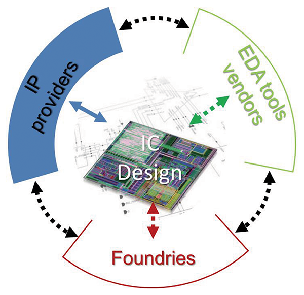
The design-enabler layer of the chip economy — the software and reusable IP that make every chip possible. A companion to Semiconductor Equipment & Materials primer.
Will Cadence Design Systems' IP segment revenue growth outpace its EDA segment growth by more than 500 basis points (5%) in FY2026?
Executive summary
Electronic design automation (EDA) and semiconductor intellectual property (IP) form the design-enabler layer of the chip industry. EDA is the software — and specialized hardware — used to design, simulate, verify, and sign off integrated circuits before they are manufactured. Semiconductor IP is pre-designed, pre-verified circuit blocks (processors, interfaces, memory controllers, analog functions) that chip designers license and reuse rather than build from scratch. Together they are the indispensable toolkit of every fabless company, IDM, and increasingly every hyperscaler designing its own silicon.
The sector is small in revenue but immense in leverage. The combined EDA-and-IP market is on the order of $20 billion a year — a fraction of the equipment market and roughly 2% of global semiconductor revenue — yet no chip reaches a fab without passing through it. That asymmetry, plus software economics, produces a remarkable financial profile: gross margins above 80%, recurring revenue of 70–80%+, customer retention above 95%, multi-year backlogs, and contractual price escalators that lift revenue from existing customers every year.
Structurally the sector is even more concentrated than equipment. EDA is a “Big Three” oligopoly — Synopsys, Cadence, and Siemens EDA — holding roughly three-quarters of the market between them. Processor IP is dominated by Arm, whose designs sit in the overwhelming majority of the world’s smartphones and a fast-growing share of data-center and automotive chips. Two forces now define the outlook: artificial intelligence (which both multiplies chip-design demand and is being embedded inside the design tools themselves), and geopolitics (the May–July 2025 episode in which the United States briefly cut China off from EDA tools demonstrated that design software is a chokepoint as potent as lithography).
1. Defining the sector and its strategic importance
EDA and IP answer a single problem: a modern system-on-chip can contain tens of billions of transistors, far beyond what any team could lay out by hand. EDA software automates the design, while IP supplies ready-made building blocks. A leading-edge processor might combine licensed CPU cores, a GPU, memory controllers, and high-speed interfaces — much of it third-party IP — stitched together and verified using tools from two or three EDA vendors.
The strategic point is leverage. The sector is often described as “small but mighty”: although EDA spending is only around 2% of the semiconductor industry’s revenue, it gates the other 98%. A fab can cost tens of billions of dollars, but it has nothing to build without a finished, verified design — and that design cannot exist without these tools. This is why EDA and IP command software-like margins and why they have become instruments of national technology policy.
Financially, the sector is also notably less cyclical than equipment and materials. Equipment demand tracks fab capital expenditure, which swings with the chip cycle; EDA and IP track customers’ R&D budgets and design activity, which are far steadier — companies keep designing through downturns. Combined with recurring-revenue contracts, this gives the sector unusually high earnings visibility.
2. Position in the value chain
In the layered view of the industry, two enabling layers sit beneath the core chip-making flow. Equipment and materials enable fabrication and packaging; IP and EDA enable design. This primer covers the latter — the layer feeding the very first stage of the chip’s life.
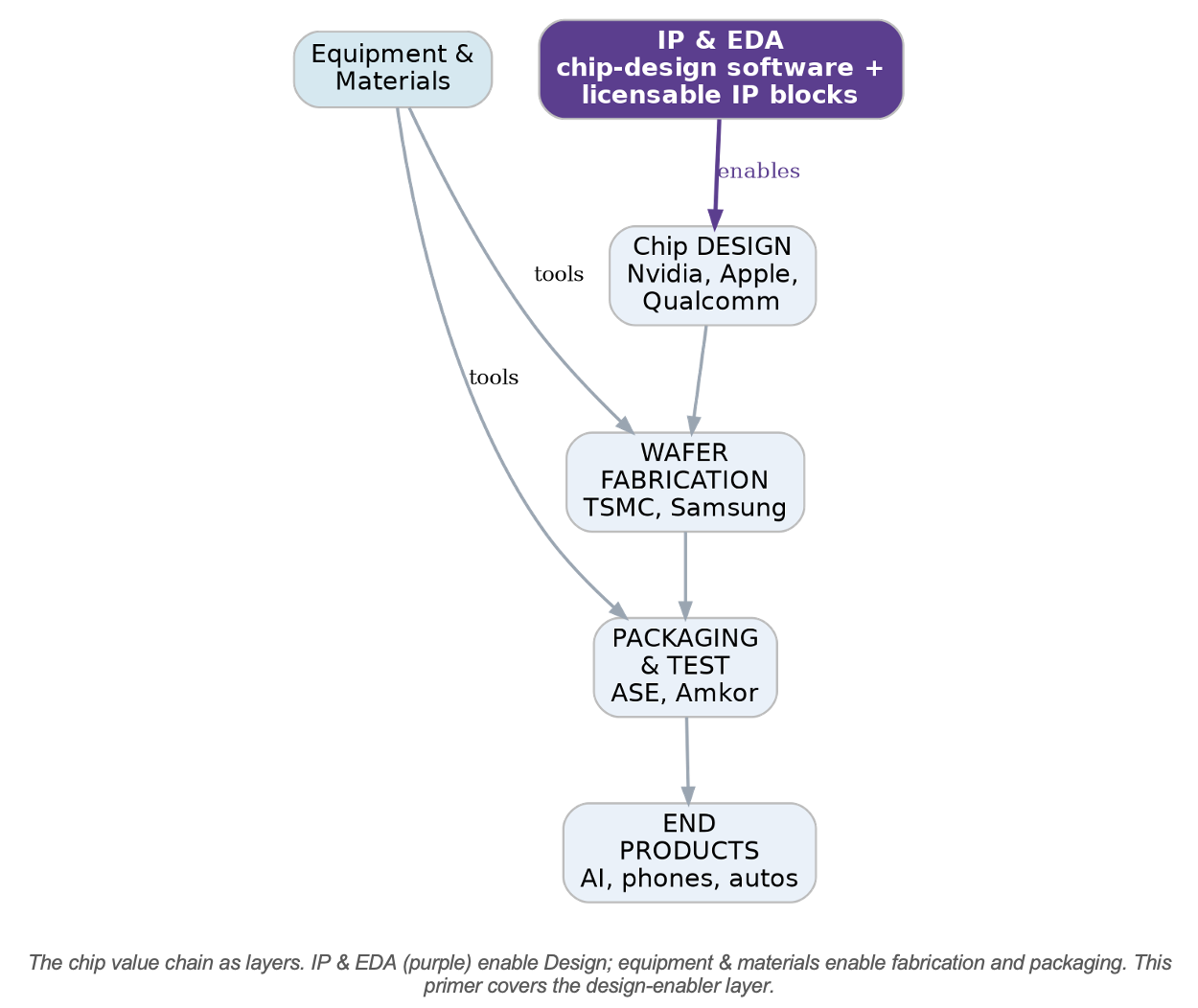
A useful contrast with the equipment sector: both are upstream enablers, but they attach to different stages and have different economics. Equipment is capital-intensive hardware sold into a cyclical capex budget; EDA and IP are capital-light software and licensing sold into steadier R&D budgets. The two also differ in customer breadth — EDA and IP serve every company that designs a chip, including fabless firms and hyperscalers that own no fabs at all.
3. The chip design flow — and where tools and IP fit
Each EDA tool category maps to a stage of the design flow, which runs from an architectural specification to “tapeout” (the point at which the finished design is sent to the foundry to make photomasks). IP blocks are inserted along the way rather than designed from scratch.
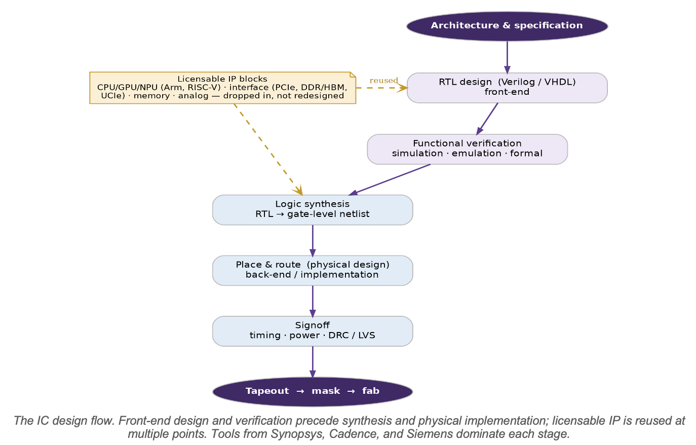
Two features of this flow drive the sector’s economics. First, verification is the single largest consumer of effort — frequently cited as 60–70% of design time — which is why simulation, emulation, and formal-verification tools (and the expensive hardware emulators that accelerate them) are such a large and profitable part of EDA. Second, the flow is sticky end-to-end: once a team builds a chip on a given vendor’s tools and qualified IP, switching mid-project risks schedule and yield, so customers rarely leave. Artificial intelligence is now compressing this flow — machine-learning optimizers can explore design options and close timing far faster than manual iteration, a capability the vendors are monetizing as a premium tier.
4. Market size and segmentation
As with equipment and materials, the two halves of this sector are best presented separately. Market-sizing also varies widely by methodology, so the figures below are indicative ranges anchored to the most authoritative tracker — SEMI’s Electronic Design Market Data (EDM) report, compiled from member-company filings.
4.1 Electronic design automation (EDA)
Core EDA — design, verification, and signoff software plus emulation/prototyping hardware — is roughly a $14–17 billion market growing at a high-single-digit to low-double-digit rate. SEMI’s EDM report, which combines EDA and IP, recorded $5.47 billion in the fourth quarter of 2025 alone (+10.3% year-on-year), implying a combined annual run-rate around $20–21 billion; computer-aided engineering (simulation/verification) was the largest single category at about $2.08 billion that quarter. Demand is broadly split across IC physical design and verification, verification/CAE, and PCB/system design.
4.2 Semiconductor IP
Licensable semiconductor IP is a smaller market — commonly estimated at $4–7 billion depending on whether processor royalties are fully counted — but it is strategically pivotal because it includes the processor architectures at the heart of most chips. The category divides into processor IP (CPU, GPU, NPU), interface IP (PCIe, USB, DDR/HBM memory, Ethernet, and the emerging UCIe chiplet interconnect), foundation IP (standard-cell libraries and memory compilers), and analog and security IP. Processor IP is the largest and most concentrated slice, dominated by Arm.
A structural quirk worth noting for analysts: in SEMI’s data the IP line is heavily influenced by a single dominant player, so reported IP “market” growth can swing with one company’s licensing timing rather than broad demand.
5. EDA tool segments and their leaders
EDA divides into several tool families, each with a clear duopoly or near-duopoly:
• Logic synthesis & digital implementation (turning RTL code into a physical layout) — Synopsys (Fusion Compiler, Design Compiler) and Cadence (Genus, Innovus).
• Verification (simulation, formal, and hardware emulation/prototyping) — the largest spend pool. Synopsys (VCS, Verdi, ZeBu) and Cadence (Xcelium, Palladium, Protium); emulation hardware is a high-value, fast-growing sub-segment driven by complex AI chips.
• Custom / analog & mixed-signal design — Cadence (Virtuoso) is the long-standing leader, with Synopsys (Custom Compiler) competing.
• Signoff (timing, power, and physical verification) — Synopsys (PrimeTime, IC Validator) and Cadence (Tempus, Voltus); Siemens EDA’s Calibre is the de facto standard in physical verification (DRC/LVS).
• PCB & system design — Cadence (Allegro), Siemens (Xpedition), with Altium and Zuken also present.
• Manufacturing / TCAD / DFM — Synopsys and Siemens; increasingly important as design and manufacturing co-optimize at advanced nodes.
6. IP segments and their leaders
• Processor IP (CPU/GPU/NPU) — dominated by Arm, whose architecture underpins essentially all smartphones and a rising share of data-center and automotive silicon. The open-standard RISC-V instruction set (commercialized by SiFive and others) is the principal long-term challenger. Synopsys (ARC) and Cadence (Tensilica) supply specialized processor and DSP cores; Imagination supplies GPU IP; Ceva supplies DSP/AI IP.
• Interface IP — high-speed connectivity (PCIe, DDR/HBM, USB, Ethernet, UCIe). Synopsys is the clear leader and this is its largest IP category; Cadence and Alphawave are significant competitors. Interface IP is booming with AI chips, which need enormous memory and chiplet bandwidth.
• Foundation, memory, analog, and security IP — standard-cell libraries and memory compilers (Arm, Synopsys), plus analog and security blocks. These are lower-profile but high-volume, deeply embedded in the foundry ecosystem.
7. Competitive structure and company financials
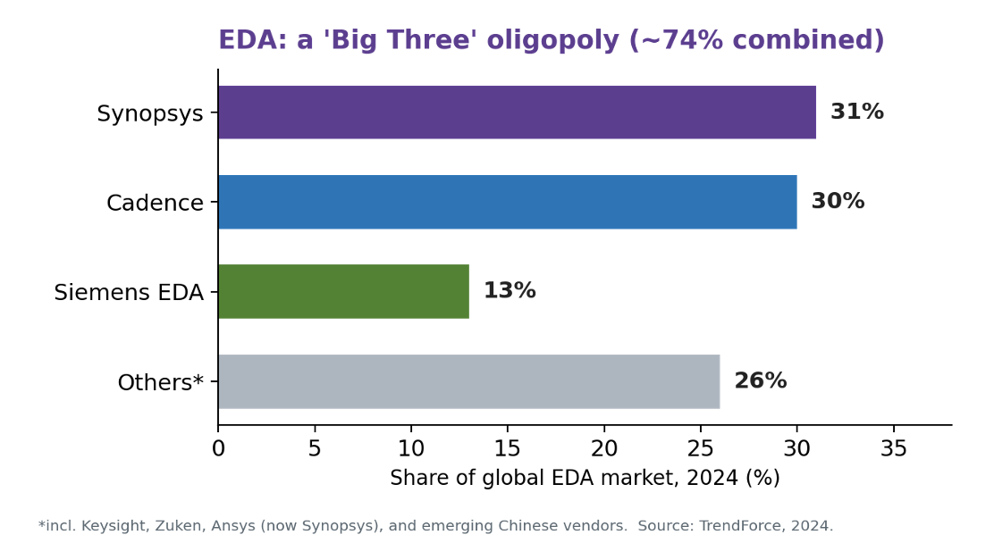
EDA is among the most concentrated software markets in existence. Per TrendForce, the three leaders held roughly Synopsys 31%, Cadence 30%, and Siemens EDA 13% in 2024 — about three-quarters of the market combined. The remainder is split among Keysight, Zuken, Ansys (now part of Synopsys), and a cohort of emerging Chinese vendors.
The financial profile across the leaders is exceptional — high growth, software margins, and large backlogs. The latest full-year results:
|
Company |
Franchise |
Latest FY
revenue |
Growth |
Note |
|
Synopsys |
EDA + Design IP (+ Ansys
simulation) |
$7.05 bn (FY25) |
+15% |
Backlog $11.4 bn; Ansys
added $0.76 bn (partial yr) |
|
Cadence |
EDA + IP (verification, custom, IP) |
~$5.3 bn (FY25) |
~+12% |
Non-GAAP op. margins ~43–44% |
|
Arm |
Processor & foundation
IP |
$4.01 bn (FY25, Mar) |
+24% |
License $1.84 bn + royalty
~$2.17 bn |
|
Siemens EDA |
EDA (Calibre, PCB, verification) |
~$2.2 bn (est.) |
— |
Unit of Siemens Digital Industries Software |
The defining corporate event was Synopsys’ $35 billion acquisition of Ansys, completed in July 2025, which extends the company from chip design into system-level simulation (thermal, electromagnetic, structural, and fluid dynamics). The logic is that modern chips cannot be designed in isolation from the systems they sit in — a 700-watt data-center GPU must be co-designed with its cooling. The deal expands Synopsys’ addressable market to roughly $31 billion and, to satisfy regulators, required divestitures (the Optical Solutions Group and PowerArtist). By mid-2025 Cadence and Synopsys each carried equity-market values around $75–80 billion — multiples that reflect their recurring revenue and moats more than their current sales.
8. Business model and economics
Two distinct monetization models operate in the sector. EDA is sold primarily through multi-year, time-based licenses — often large enterprise license agreements (ELAs) — supplemented by upfront emulation-hardware sales. IP is sold through a combination of upfront license fees and per-unit royalties collected for the life of the chip.
The EDA model is, in effect, a renewal engine. Time-based arrangements are 70–83% of Synopsys’ and Cadence’s revenue; customer retention exceeds 95% (and approaches 99% for signoff and analog tools); and contracts carry annual escalators, so a customer that signed a $10 million ELA in 2020 may renew at $12–14 million in 2025 without adding a single engineer. The result is large committed backlogs — Synopsys reported $11.4 billion (about 1.6 years of revenue) and Cadence roughly $7.8 billion — giving rare forward visibility for a technology business.
Arm’s IP model has a characteristic time lag that rewards patient analysis:
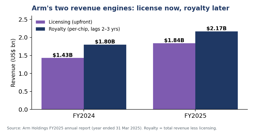
Because royalties lag licenses by two to three years, a surge in licensing today is an advance signal of royalty growth in 2027–28. Arm is also raising revenue per chip: its newer Armv9 architecture and pre-integrated Compute Subsystems (CSS) carry higher royalty rates than prior generations, and v9 already accounts for roughly a third of royalties. Annualized contract value (ACV) — a normalized measure of the licensing base — was growing around 28% year-on-year as of late 2025.
9. Demand drivers
Artificial intelligence — a double tailwind. AI raises demand in two ways. It multiplies the number and complexity of chips being designed (accelerators, networking, custom silicon), and it is being embedded inside the EDA tools themselves: ML-driven optimizers such as Synopsys’ DSO.ai and Cadence’s Cerebrus can close designs faster and better than manual methods, which the vendors sell as a high-margin premium.
Rising design complexity. Each new node (3nm, 2nm, gate-all-around) and each additional billion transistors increases verification and implementation effort, lifting tool consumption per design.
Chiplets, 3D-IC, and advanced packaging. Multi-die designs require new tools for partitioning, 3D floor-planning, thermal analysis, and die-to-die interconnect — a direct beneficiary of the same advanced-packaging wave reshaping the back-end, and a key motivation for the Synopsys-Ansys combination.
The custom-silicon boom. Hyperscalers designing their own chips (Google’s TPU, AWS’s Graviton and Trainium, Microsoft’s Maia, Meta’s MTIA) have multiplied the number of sophisticated design starts — each one a new consumer of EDA seats and licensed IP, often from customers who never previously designed silicon.
10. Geopolitics: design software as a chokepoint
EDA is a control point comparable to EUV lithography: the leading tools are supplied by two US companies and one US-based unit of a German firm, and they cannot be readily substituted. This was demonstrated vividly in 2025. On 23–29 May 2025, the US Bureau of Industry and Security imposed license requirements on EDA exports to China, abruptly cutting Chinese chip designers off from new tools, updates, and support. Barely six weeks later, on 2–3 July 2025, the restrictions were rescinded as part of a broader US-China framework that also eased China’s rare-earth export curbs.
The episode underscored several realities. China was a meaningful revenue source — roughly 16% of Synopsys and ~12% of Cadence revenue — so the controls hurt the vendors as well as their customers, and Siemens EDA reported a significant China revenue decline that quarter. It also accelerated China’s push for domestic EDA (Empyrean, Primarius, X-EPIC, and newer entrants such as Univista), though Chinese tools remain far behind on full-flow, leading-edge design. RISC-V adds a parallel dimension: as an open, license-free instruction set not owned by any single country’s company, it is attractive to Chinese designers seeking to reduce dependence on Arm.
Will US-headquartered EDA vendors see their total revenue share from the Asia-Pacific region (excluding Japan) drop below 20% in audited fiscal year 2026?
11. A framework for financial analysis
• Value the recurring base and backlog. Time-based revenue mix, retention rates, and committed backlog (e.g., Synopsys’ $11.4 bn) are the core quality signals; they make revenue unusually predictable.
• For Arm, watch licensing as a leading indicator. Licensing and ACV today foreshadow royalties two to three years out; royalty-per-chip (the v9 and CSS mix) is the key margin lever.
• Track the AI attach rate. Adoption of AI-driven tools (DSO.ai, Cerebrus) is both a growth driver and a test of pricing power.
• Remember the sector is R&D-cycle, not capex-cycle. EDA/IP revenue is tied to customers’ design budgets, which are steadier than fab capital spending — a defensive quality versus the equipment names.
• Mind valuation. These are high-multiple equities; much of the value rests on durable growth and moats, so they are sensitive to any deceleration or to regulatory and geopolitical shocks.
PredictionMarkets Org disclaimer: This article is an educational overview, not investment advice, and does not constitute a recommendation to buy or sell any security.
12. Key debates to watch
• RISC-V versus Arm. Whether the open instruction set erodes Arm’s royalty economics in volume markets, or remains complementary at the edges.
• Arm moving up the stack. Arm’s shift toward pre-integrated subsystems (CSS) — and reports of its own chips — raises potential channel conflict with the customers it licenses to.
• AI in EDA: boon or pricing pressure? Whether AI tools mainly expand the premium tier, or eventually let customers do more with fewer seats.
• China’s domestic EDA. How quickly local vendors can close the gap on full-flow, leading-edge design — the sector’s equivalent of the EUV question.
• Concentration and antitrust. The Synopsys-Ansys deal required divestitures; further consolidation will draw scrutiny.
13. Risk summary
• Geopolitical/regulatory — export controls can cut off a ~10–16% revenue market overnight, as 2025 showed.
• Disruption risk — RISC-V (to Arm) and open-source EDA efforts (to the Big Three), though both remain early.
• Customer concentration and consolidation — a handful of large designers and foundries drive much of demand.
• Valuation/multiple risk — rich multiples leave little room for growth disappointment.
• Integration risk — absorbing Ansys is a large undertaking for Synopsys.