Where chips become products — and the demand that pulls the whole chain
Will Hyperscalers raise their capex target again in upcoming quarterly results (Jul-Aug 2026)?
YesResult
0.00%
NoResult
0.00%
0 Polls
Ended
Executive summary
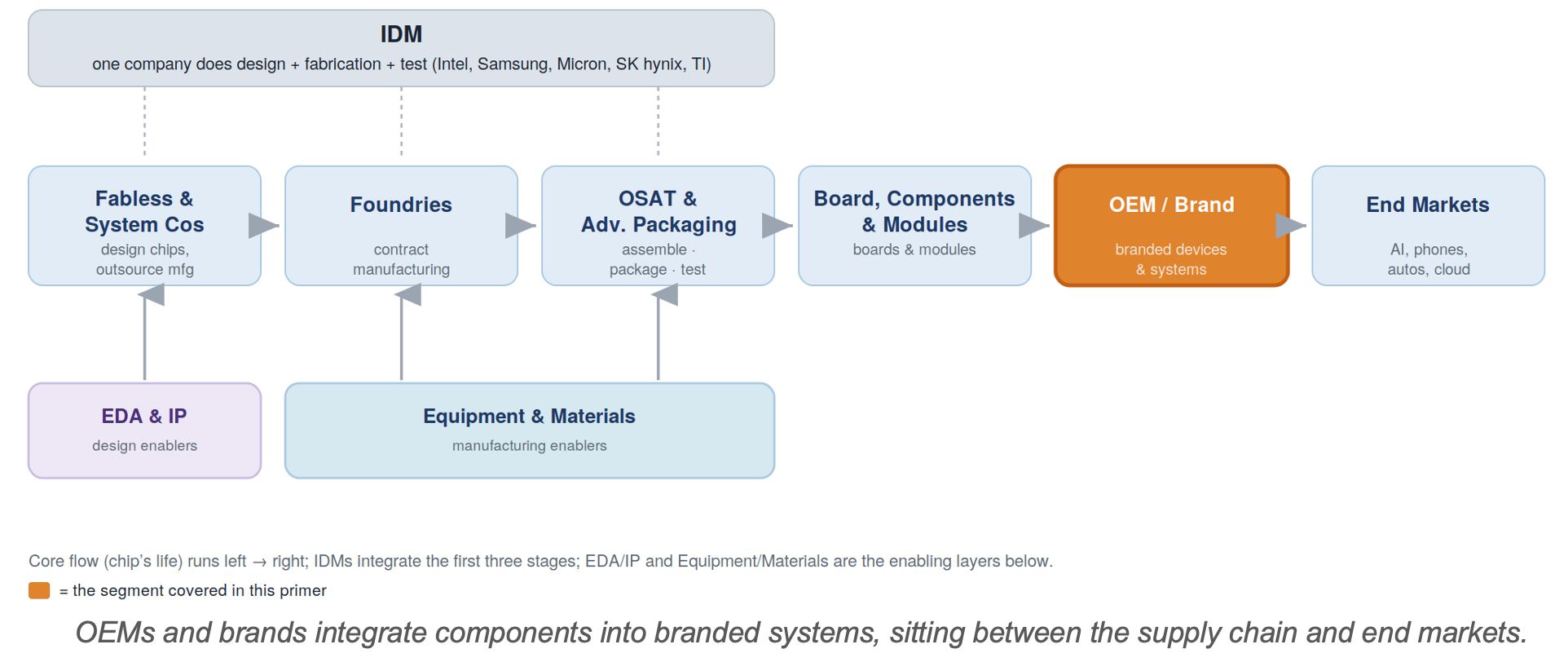
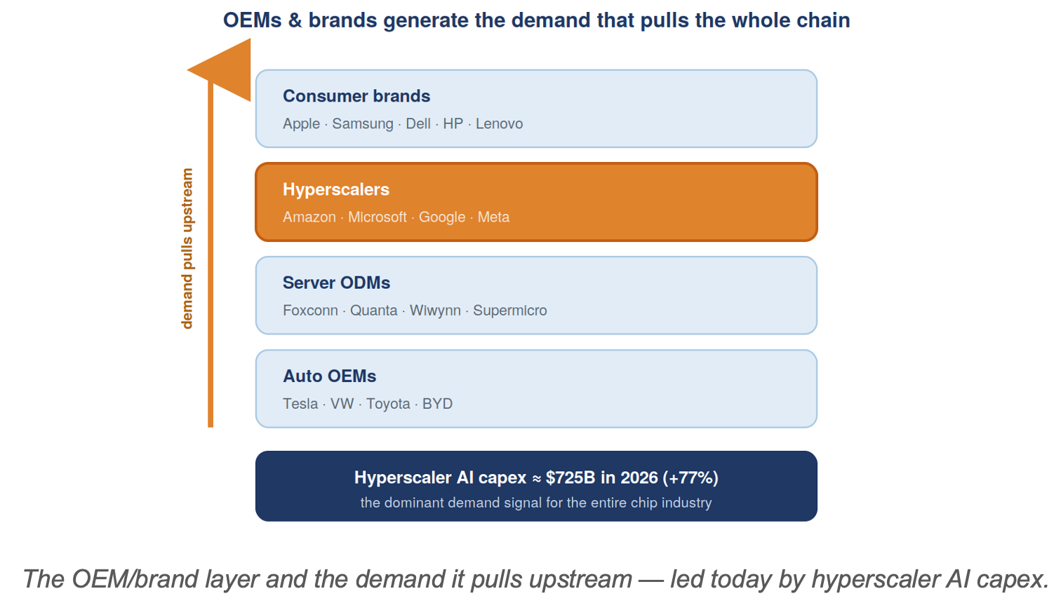
OEMs and brands are where chips become products — the device makers, server builders, and system companies that integrate semiconductors into things people and businesses buy. They are the origin of demand that pulls silicon through the entire value chain. The category spans consumer-device brands (Apple, Samsung, Dell, HP, Lenovo), data-center server ODMs (Foxconn, Quanta, Wiwynn, Supermicro), automakers, and — most importantly today — the hyperscalers whose AI-infrastructure spending now drives the cycle.
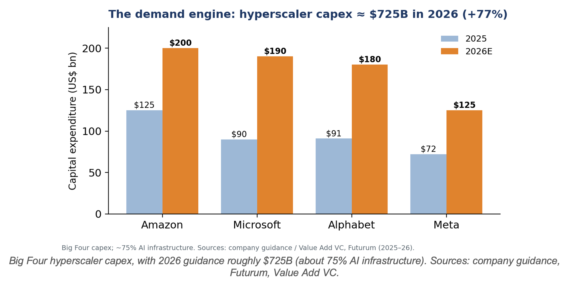
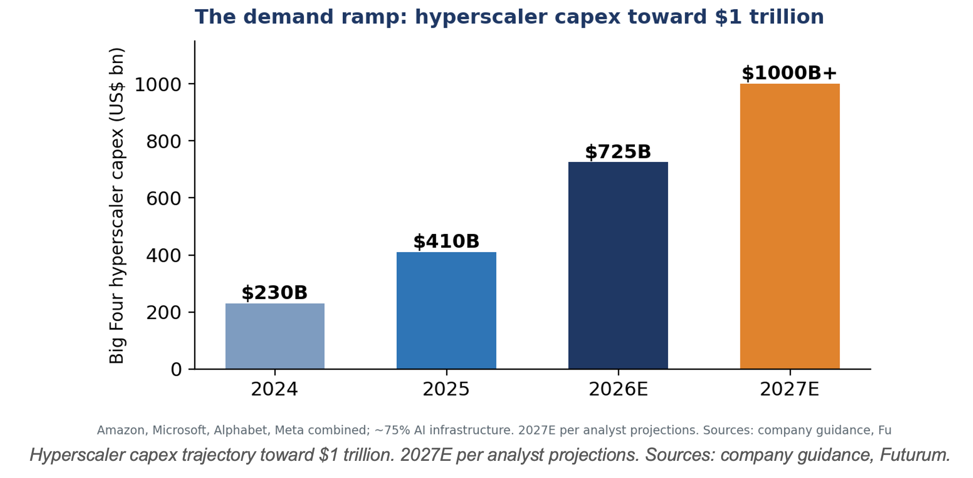
That demand signal is staggering: the four largest US hyperscalers are guiding to roughly $725 billion of capital expenditure in 2026, up about 77% from ~$410 billion in 2025, the overwhelming majority of it AI infrastructure, with analysts projecting big-tech capex above $1 trillion by 2027. This is the engine behind the foundry, fabless, memory, and packaging booms described in the companion primers.
1. Definition and strategic importance
OEMs (original equipment manufacturers) and brands sit at the downstream end of the chain, buying chips, boards, modules, and components and assembling them into finished systems sold under a brand to end markets. They matter because demand starts here — every wafer TSMC makes and every tool ASML sells exists ultimately to satisfy an order that originates with an OEM or a hyperscaler.
2. Position in the value chain
A key nuance: the line between “brand” and “chip designer” is blurring. Apple and the hyperscalers now design their own silicon (covered in the Fabless primer), making them simultaneously the demand origin and an upstream design participant — a vertical integration reshaping the industry’s balance of power.
3. Structure: brands, ODMs, and hyperscalers
Consumer-device brands. Apple, Samsung, Dell, HP, Lenovo, Xiaomi and others design and sell branded phones, PCs, and electronics, capturing brand margin and owning the customer — often outsourcing physical assembly to contract manufacturers (e.g., Foxconn for Apple).
Server and data-center ODMs. The AI build-out is physically assembled by original design manufacturers — Foxconn (Hon Hai), Quanta, Wiwynn, Wistron, and Supermicro — which build the servers and racks that house GPUs and accelerators. These are high-volume, thin-margin businesses booming on AI orders.
Hyperscalers. Amazon, Microsoft, Google, and Meta are both the largest buyers of AI hardware and increasingly the designers of their own chips. Their capital spending is the dominant demand variable for the entire semiconductor industry today.
4. The demand engine: hyperscaler capital spending
The trajectory matters as much as the level: spending has roughly doubled each year and is projected to approach $1 trillion in 2027, with the five largest US hyperscalers reportedly planning to add around $2 trillion of AI-related assets by 2030.
5. Competitive structure and key players
The layer divides by role rather than by a single revenue ranking; margins differ sharply between brand owners and contract builders.
Category
Examples
Role in the
chain
Device brands
Apple, Samsung, Dell, HP,
Lenovo
Design/sell branded devices;
own the end customer; rich margins
Hyperscalers
Amazon, Microsoft, Google, Meta
Largest AI-hardware buyers; also design custom silicon
Server ODMs
Foxconn, Quanta, Wiwynn,
Supermicro
Build AI servers and racks
(thin-margin, high-volume)
Auto OEMs
Tesla, VW, Toyota, BYD
Rising semiconductor content per vehicle
6. Business model and economics
Economics vary enormously by role. Brand owners like Apple capture high margins by owning design, software, and the customer relationship, while contract ODMs (Foxconn, Quanta) run on razor-thin margins despite enormous revenue. Hyperscalers are not selling hardware at all — their chip and server spending is a cost of delivering cloud and AI services, which is why the return on that capex is so closely scrutinized.
7. Demand drivers
• AI infrastructure build-out. Hyperscaler capex (~$725B in 2026) is the single largest pull on advanced logic, memory, and packaging.
• Device refresh cycles. AI PCs and AI smartphones, plus normal replacement of the ~1.2 billion phones and ~250 million PCs shipped each year, provide a large volume base.
• Automotive content. Electrification and ADAS keep raising the dollar value of chips per vehicle.
8. Geopolitics and strategic dimension
OEMs sit atop globally distributed supply chains exposed to tariffs, export controls, and reshoring pressure. Device assembly is shifting (e.g., toward India and Vietnam); AI-server supply chains concentrate in Taiwan-linked ODMs; and the hyperscalers’ build-out is increasingly constrained not by chips but by power and data-center construction — the emerging physical bottleneck of the AI era.
9. A framework for financial analysis
• Follow the capex guidance. Hyperscaler capital-spending guidance is the leading indicator for the whole semiconductor cycle — watch it above almost anything else.
• Separate brand from contract economics. Apple’s margins and a server ODM’s are not comparable despite both being “OEMs.”
• Watch the ROI question. Whether AI revenue justifies the capex is the debate that could move the entire chain.
• Track the physical constraints. Power availability and data-center construction timelines increasingly gate demand.
10. Key debates
• Is the AI capex sustainable? Whether ~$725B+ of annual investment generates adequate returns — the industry’s biggest open question; a pullback would ripple through every upstream segment.
• Vertical integration. How far OEMs and hyperscalers take in-house silicon, eroding the merchant-chip market.
• Demand concentration. Whether reliance on a handful of hyperscalers makes the cycle more fragile.
11. Risk summary
• AI-capex sustainability — the dominant risk; valuations across the chain embed continued spending.
• Demand concentration — a few hyperscalers drive much of leading-edge demand.
• Margin asymmetry — contract ODMs are structurally low-margin and exposed.
• Physical constraints — power and construction bottlenecks; supply-chain and tariff exposure.
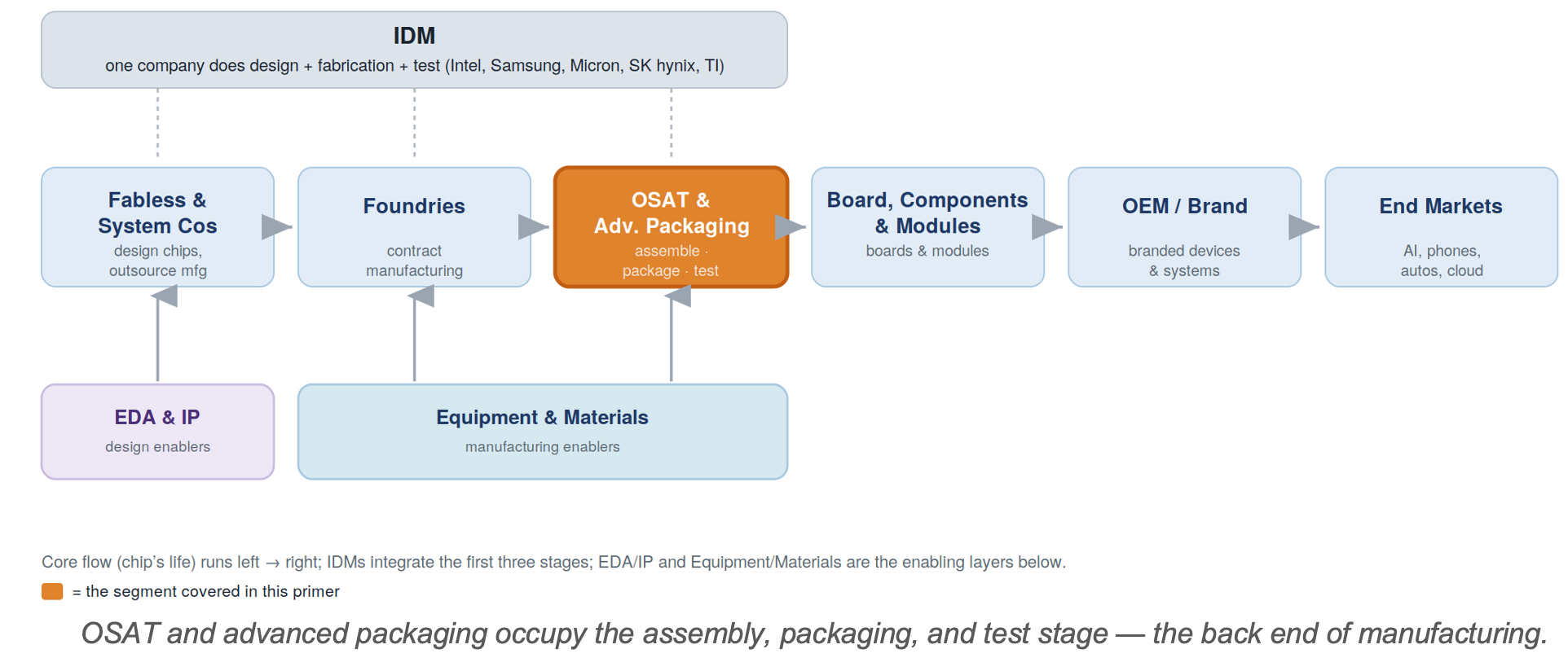
Assembly, test, and the packaging revolution reshaping the back end
Executive summary
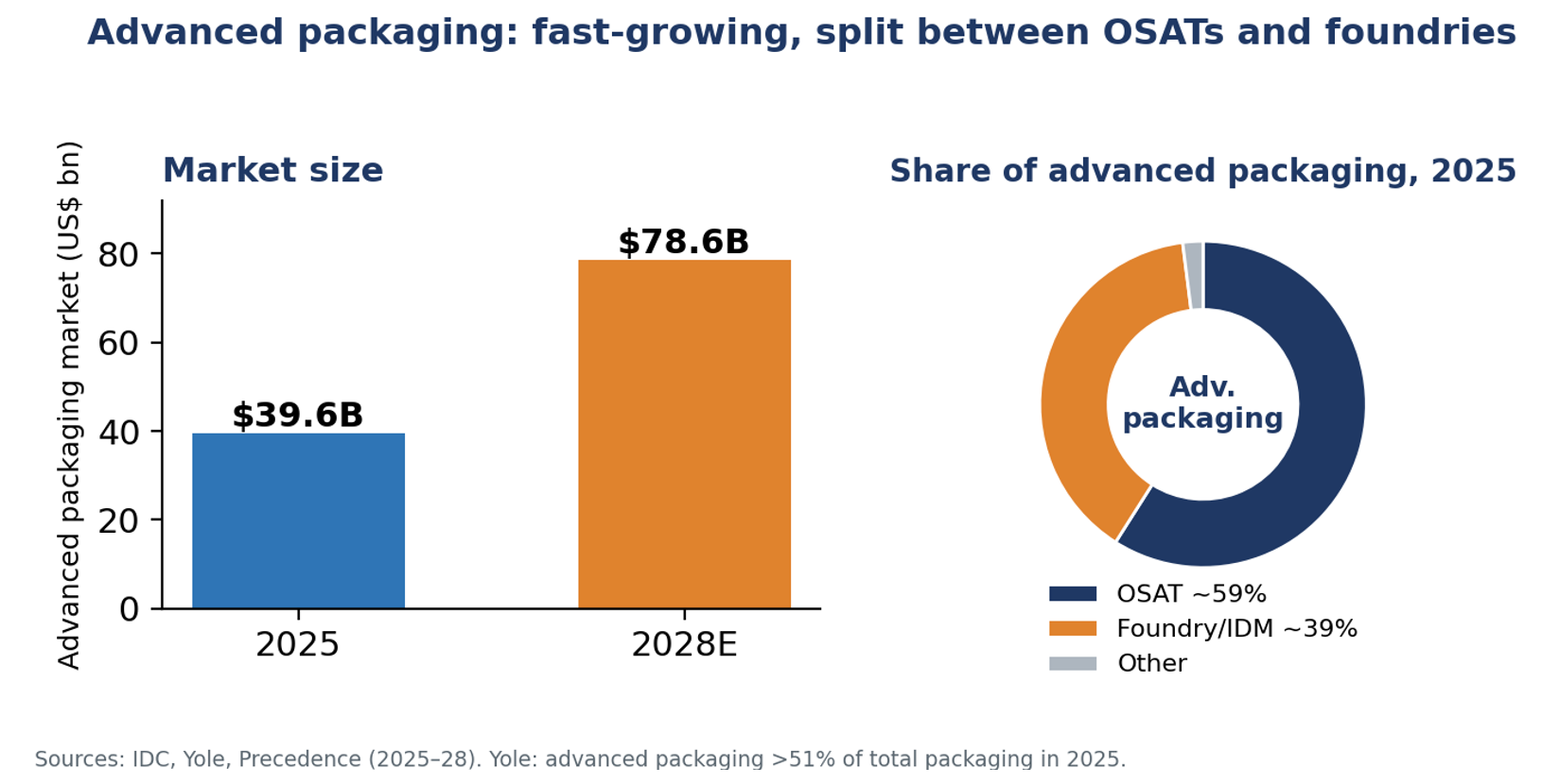
OSAT — outsourced semiconductor assembly and test — firms take finished wafers and turn them into packaged, tested chips. Historically the lowest-margin link in the chain, the back end has been transformed by advanced packaging: chiplets, 2.5D/3D stacking, hybrid bonding, and platforms like TSMC’s CoWoS that are essential to AI chips. The advanced-packaging market is growing from roughly $40 billion in 2025 toward ~$79 billion by 2028.
The competitive twist is that this lucrative new work is contested by three groups: the OSATs (ASE, Amkor, JCET), the foundries (TSMC), and the IDMs (Intel, Samsung). OSATs hold roughly 59% of advanced packaging and the foundry/IDM group about 39% — and the foundries are pushing in hard, because advanced packaging increasingly uses wafer-level, fab-style processes that blur the old front-end/back-end line.
1. Defining the sector and its strategic importance
After a wafer leaves the fab, it must be diced into individual dies, connected and protected within a package, and tested. OSATs provide these back-end services under contract, just as foundries provide front-end manufacturing. Once an afterthought, packaging is now a primary determinant of chip performance — which has turned the back end into a strategic battleground.
2. Position in the value chain
As noted in the Equipment primer, the OSAT service sits here in the chain, while the equipment used to perform it is upstream. Advanced packaging is now drawing front-end tools into the back end — the central structural shift in this segment.
3. Structure: from traditional assembly to advanced packaging
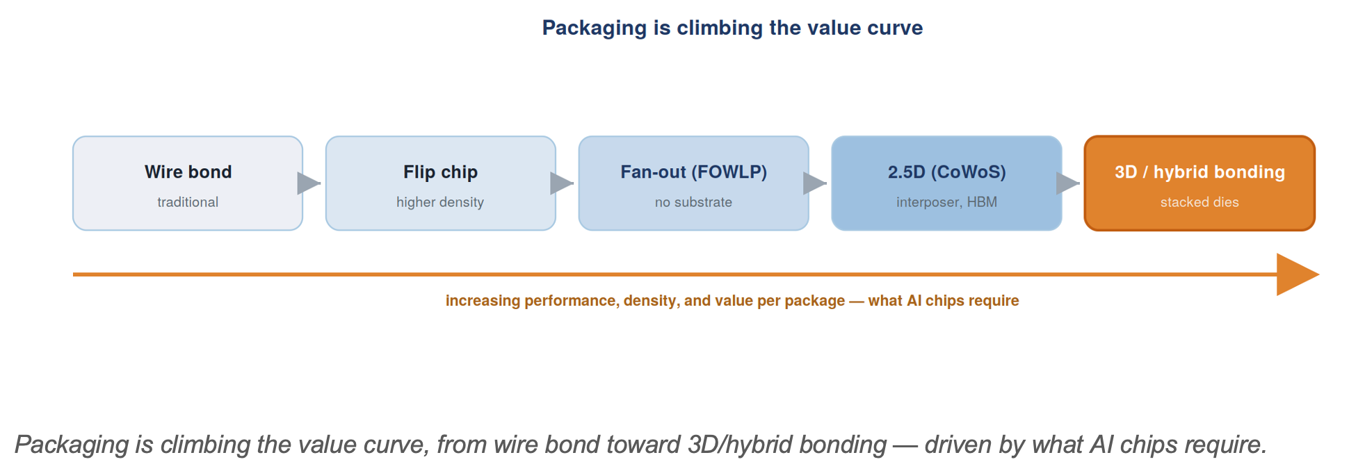
Traditional OSAT. High-volume wire-bond and flip-chip assembly and test for the bulk of the world’s chips — a thin-margin, scale-and-cost business (Amkor’s gross margin runs around 15%, a world away from foundry economics).
Advanced packaging. The high-value frontier: 2.5D/3D integration, chiplets, fan-out, and hybrid bonding that connect multiple dies and stacked HBM into one high-performance package. This is what AI accelerators require, and by some estimates it surpassed traditional packaging as a majority of total packaging value in 2025.
The players. ASE is the world’s largest OSAT (with a large electronics-manufacturing arm alongside assembly/test); Amkor is second and JCET is China’s leader, followed by Powertech, TFME, and test specialists such as KYEC. But TSMC (CoWoS, SoIC), Samsung (I-Cube, X-Cube), and Intel (Foveros, EMIB) now perform much of the cutting-edge packaging themselves.
4. Market size and segmentation
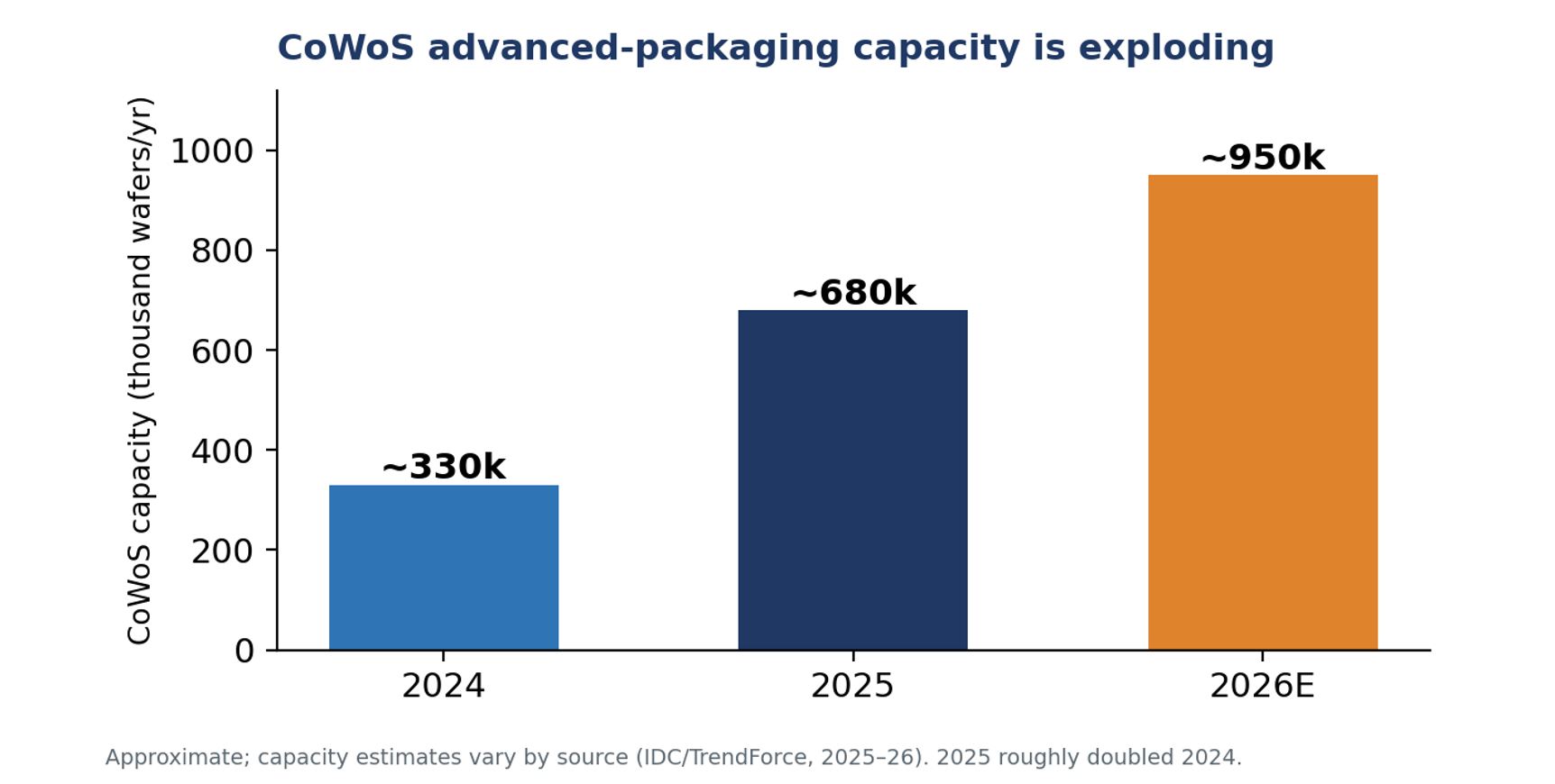
The growth is concentrated in AI-related advanced packaging, and the single most-watched capacity metric is TSMC’s CoWoS, which has roughly doubled year-on-year.
5. Competitive structure and company financials
OSATs are scaled but thin-margin; the foundry/IDM camp is capturing the most advanced (and most profitable) packaging.
Company
Position
Scale
Note
ASE Technology
#1 OSAT
~$20B group revenue
Advanced-packaging sales
~$1B in 2025; includes SPIL and an EMS arm
~680k CoWoS wafers in 2025; allocates to Nvidia, Google, others
6. Business model and economics
Traditional OSAT is a high-volume, low-margin business: gross margins in the mid-teens, competing on cost, scale, and geographic footprint. Advanced packaging offers a path to better economics, but it requires heavy investment in wafer-level, fab-style equipment — which is precisely why the better-capitalized foundries can compete for it. The result is margin pressure from both ends: commodity assembly below, foundry encroachment above.
7. Demand drivers
• AI and HBM. Stacking logic with high-bandwidth memory and integrating chiplets is the core of advanced-packaging demand.
• The end of easy scaling. As transistor shrinks get harder, more performance comes from packaging — structurally favouring this segment.
• CoWoS allocation. TSMC’s packaging capacity gates AI-GPU supply, with 2026 allocations reportedly reserved for Google’s TPU, Meta, OpenAI, and others.
8. Geopolitics and strategic dimension
Packaging has become a reshoring priority: the US CHIPS Act funds back-end capacity (Amkor’s ~$2 billion Arizona plant, with a 10-year TSMC agreement), and Europe is supporting its own. The US-China contest is also reshaping OSAT customer allocation, with Western firms diversifying away from China-based assemblers toward Vietnam, Taiwan, and the US. JCET and other Chinese OSATs, meanwhile, anchor a parallel domestic supply chain.
9. A framework for financial analysis
• Distinguish traditional from advanced. Advanced-packaging mix and growth are the value drivers; traditional assembly is a thin-margin base.
• Watch capex and utilization. A back-end capacity race raises overbuild risk; utilization is the cyclical signal.
• Track foundry encroachment. How much advanced packaging TSMC and Samsung keep in-house caps the OSAT opportunity.
• Mind margins. OSAT returns are structurally lower than foundries’ — advanced packaging is the path up, not a guarantee.
10. Key debates
• Who captures advanced-packaging value? OSATs versus foundries (TSMC) versus IDMs — the segment’s defining contest.
• Overbuild risk. Whether the simultaneous capacity race produces a glut in 2026–27.
• Hybrid bonding leadership. Which players master sub-10-micron hybrid bonding at high yield.
11. Risk summary
• Thin margins — structural, especially in traditional assembly.
• Foundry encroachment — TSMC capturing the most profitable packaging in-house.
The contract chip manufacturers — and TSMC’s extraordinary dominance.
What will TSMC's 3Q2026 operating margin be (guided 56-58%)?
<56%Result
0.00%
56-58%Result
0.00%
>58%Result
100.00%
1 Polls
EndedTBD
Executive summary
Foundries are pure-play contract chip manufacturers: they fabricate chips designed by others and own no end-product IP. Their existence is what makes the fabless model possible. The segment is defined by one company’s dominance — TSMC, with roughly 70% of global foundry revenue and an even larger share at the leading edge — arguably the single most strategically important company in technology. TSMC’s 2025 revenue reached $122.4 billion (+36%) at a 59.9% gross margin, and it guided 2026 capital spending of $52–56 billion.
Behind TSMC, Samsung Foundry (a distant second, hampered by yield issues), China’s SMIC (growing despite export controls), and the mature-node specialists UMC and GlobalFoundries compete in a far less profitable tier. Intel Foundry is a heavily funded but still nascent challenger. The economics at the leading edge are brutal in capital but, for TSMC, exceptional in pricing power — its 2nm wafers reportedly price around $30,000 each.
1. Defining the sector and its strategic importance
A foundry sells manufacturing capacity and process technology, not products. Customers — fabless firms, IDMs, and system companies — send designs to be fabricated at an agreed price per wafer. Because virtually all advanced chips in the world are made by a handful of foundries (and overwhelmingly by TSMC), the segment is the physical chokepoint of the entire digital economy and the focal point of industrial policy.
2. Position in the value chain
TSMC’s moat is built from process leadership, manufacturing yield, the breadth of its design ecosystem (IP, EDA support, and advanced packaging), and sheer scale — each reinforcing the others. Leading customers co-develop on its newest node, which funds the next node, which attracts the next generation of customers.
Companies that design and manufacture their own chips — memory, analog, power, and Intel.
Executive summary
Integrated device manufacturers (IDMs) both design and manufacture their own chips — the original structure of the semiconductor industry, predating the split into fabless designers and contract foundries. IDMs own fabs, control their process technology, and sell finished products under their own brand. They persist because, in their domains, product and process are inseparable. Today they fall into three families: memory (Samsung, SK hynix, Micron), analog/power/embedded (Texas Instruments, Analog Devices, Infineon, ST, NXP, Microchip, Renesas), and logic (Intel, now pivoting toward a foundry model).
The defining dynamic of the current cycle is the AI-driven memory supercycle. High-bandwidth memory (HBM) has transformed DRAM from a boom-bust commodity into a constrained, premium, strategically vital product — so much so that in 2025 SK hynix overtook Samsung in both DRAM revenue and, for the first time ever, operating profit. The analog/power family, by contrast, offers steadier, less cyclical growth tied to automotive and industrial electronics, while Intel’s foundry transition is one of the industry’s biggest open questions.
1. Defining the sector and its strategic importance
An IDM performs the entire chip lifecycle in-house: design, wafer fabrication, and assembly/test. This is the opposite of the disaggregated model, in which a fabless company designs and a foundry manufactures. IDMs remain vertically integrated where manufacturing know-how is itself the competitive advantage — the recipe for a DRAM cell or a precision data converter lives in the process, not in a licensable design file.
Their strategic weight is large: IDMs own the memory that every AI accelerator needs, the analog and power chips in every car and factory, and — through Intel — a substantial share of Western leading-edge manufacturing capacity. They also carry the heaviest financial burden in the industry, funding both R&D and multi-billion-dollar fabs.
2. Position in the value chain
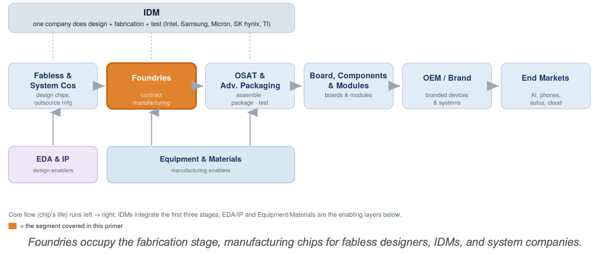
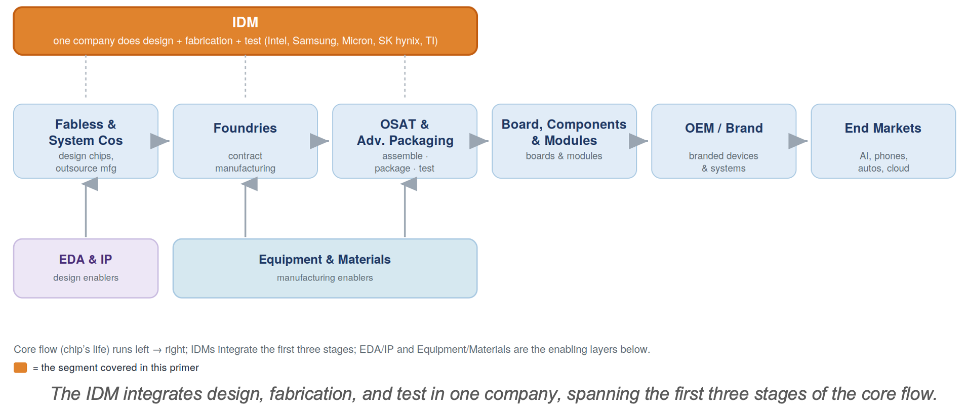
In the value-chain map, an IDM effectively spans the first three stages — design, fabrication, and test — within a single company, rather than handing the chip between specialist firms.
This integration is increasingly the exception rather than the rule. Leading-edge logic largely abandoned it (fabless + foundry), and even some IDMs now outsource their most advanced nodes to TSMC while keeping mature production in-house — a “fab-lite” hybrid. Memory and analog remain the strongholds of full integration.
3. The three families of IDMs
IDMs are not one business but three, with very different economics. (This corrects a framing point: there are three families, not two — memory, analog/power/embedded, and logic.)
The design-enabler layer of the chip economy — the software and reusable IP that make every chip possible. A companion to Semiconductor Equipment & Materials primer.
Will Cadence Design Systems' IP segment revenue growth outpace its EDA segment growth by more than 500 basis points (5%) in FY2026?
YesResult
92.31%
NoResult
7.69%
13 Polls
EndedTBD
Executive summary
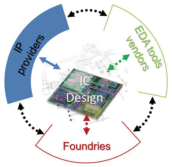
Electronic design automation (EDA) and semiconductor intellectual property (IP) form the design-enabler layer of the chip industry. EDA is the software — and specialized hardware — used to design, simulate, verify, and sign off integrated circuits before they are manufactured. Semiconductor IP is pre-designed, pre-verified circuit blocks (processors, interfaces, memory controllers, analog functions) that chip designers license and reuse rather than build from scratch. Together they are the indispensable toolkit of every fabless company, IDM, and increasingly every hyperscaler designing its own silicon.
The sector is small in revenue but immense in leverage. The combined EDA-and-IP market is on the order of $20 billion a year — a fraction of the equipment market and roughly 2% of global semiconductor revenue — yet no chip reaches a fab without passing through it. That asymmetry, plus software economics, produces a remarkable financial profile: gross margins above 80%, recurring revenue of 70–80%+, customer retention above 95%, multi-year backlogs, and contractual price escalators that lift revenue from existing customers every year.
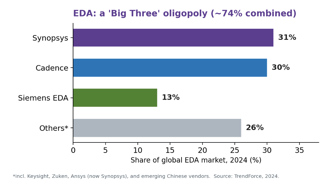
Structurally the sector is even more concentrated than equipment. EDA is a “Big Three” oligopoly — Synopsys, Cadence, and Siemens EDA — holding roughly three-quarters of the market between them. Processor IP is dominated by Arm, whose designs sit in the overwhelming majority of the world’s smartphones and a fast-growing share of data-center and automotive chips. Two forces now define the outlook: artificial intelligence (which both multiplies chip-design demand and is being embedded inside the design tools themselves), and geopolitics (the May–July 2025 episode in which the United States briefly cut China off from EDA tools demonstrated that design software is a chokepoint as potent as lithography).
1. Defining the sector and its strategic importance
EDA and IP answer a single problem: a modern system-on-chip can contain tens of billions of transistors, far beyond what any team could lay out by hand. EDA software automates the design, while IP supplies ready-made building blocks. A leading-edge processor might combine licensed CPU cores, a GPU, memory controllers, and high-speed interfaces — much of it third-party IP — stitched together and verified using tools from two or three EDA vendors.
The strategic point is leverage. The sector is often described as “small but mighty”: although EDA spending is only around 2% of the semiconductor industry’s revenue, it gates the other 98%. A fab can cost tens of billions of dollars, but it has nothing to build without a finished, verified design — and that design cannot exist without these tools. This is why EDA and IP command software-like margins and why they have become instruments of national technology policy.
Financially, the sector is also notably less cyclical than equipment and materials. Equipment demand tracks fab capital expenditure, which swings with the chip cycle; EDA and IP track customers’ R&D budgets and design activity, which are far steadier — companies keep designing through downturns. Combined with recurring-revenue contracts, this gives the sector unusually high earnings visibility.
2. Position in the value chain
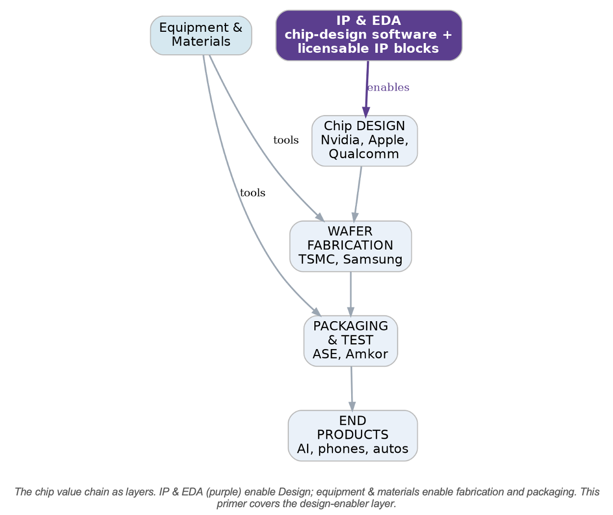
In the layered view of the industry, two enabling layers sit beneath the core chip-making flow. Equipment and materials enable fabrication and packaging;IP and EDA enable design. This primer covers the latter — the layer feeding the very first stage of the chip’s life.
A useful contrast with the equipment sector: both are upstream enablers, but they attach to different stages and have different economics. Equipment is capital-intensive hardware sold into a cyclical capex budget; EDA and IP are capital-light software and licensing sold into steadier R&D budgets. The two also differ in customer breadth — EDA and IP serve every company that designs a chip, including fabless firms and hyperscalers that own no fabs at all.
3. The chip design flow — and where tools and IP fit
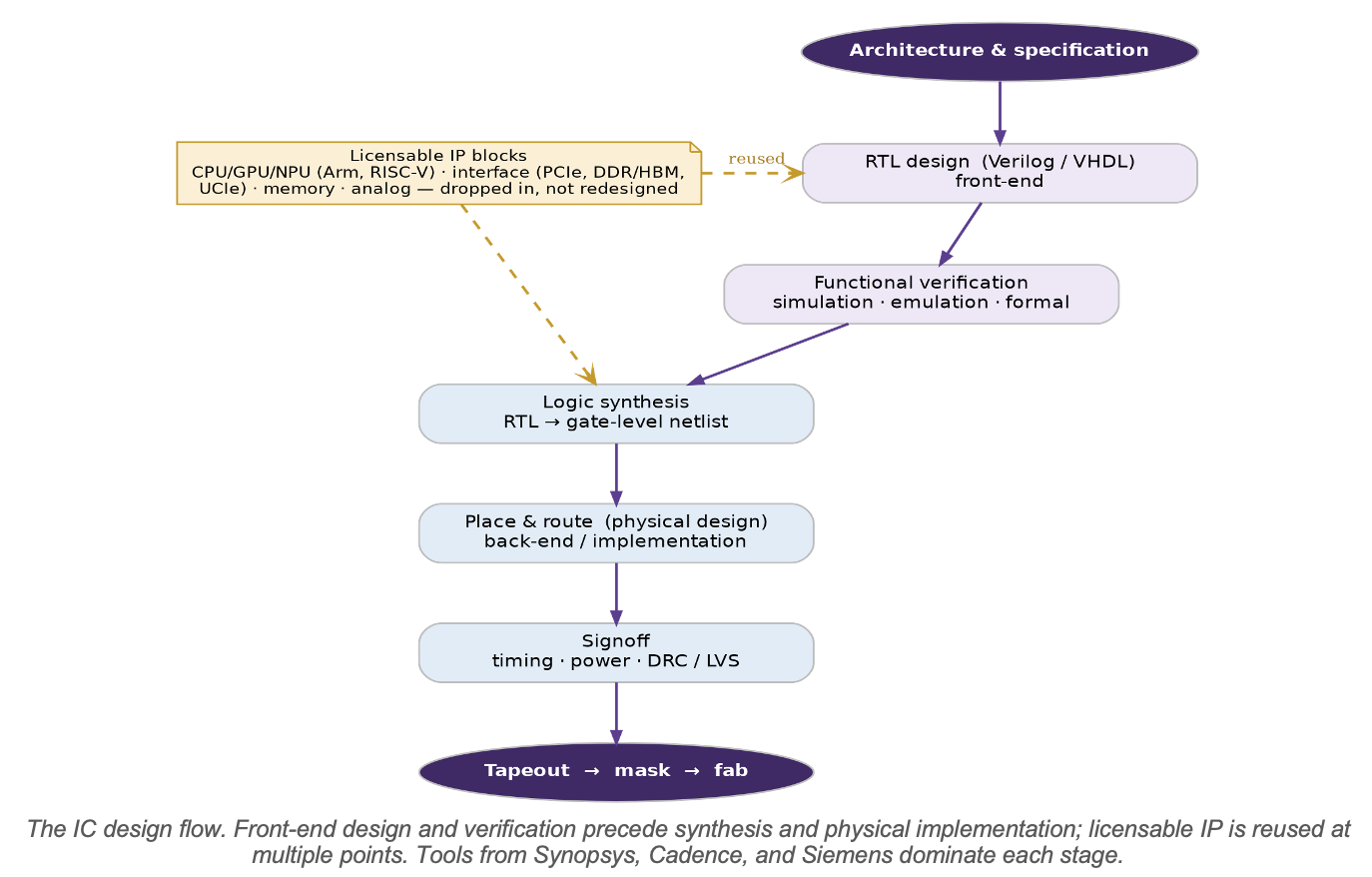
Each EDA tool category maps to a stage of the design flow, which runs from an architectural specification to “tapeout” (the point at which the finished design is sent to the foundry to make photomasks). IP blocks are inserted along the way rather than designed from scratch.
Two features of this flow drive the sector’s economics. First, verification is the single largest consumer of effort — frequently cited as 60–70% of design time — which is why simulation, emulation, and formal-verification tools (and the expensive hardware emulators that accelerate them) are such a large and profitable part of EDA. Second, the flow is sticky end-to-end: once a team builds a chip on a given vendor’s tools and qualified IP, switching mid-project risks schedule and yield, so customers rarely leave. Artificial intelligence is now compressing this flow — machine-learning optimizers can explore design options and close timing far faster than manual iteration, a capability the vendors are monetizing as a premium tier.
4. Market size and segmentation
As with equipment and materials, the two halves of this sector are best presented separately. Market-sizing also varies widely by methodology, so the figures below are indicative ranges anchored to the most authoritative tracker — SEMI’s Electronic Design Market Data (EDM) report, compiled from member-company filings.
4.1 Electronic design automation (EDA)
Core EDA — design, verification, and signoff software plus emulation/prototyping hardware — is roughly a $14–17 billion market growing at a high-single-digit to low-double-digit rate. SEMI’s EDM report, which combines EDA and IP, recorded $5.47 billion in the fourth quarter of 2025 alone (+10.3% year-on-year), implying a combined annual run-rate around $20–21 billion; computer-aided engineering (simulation/verification) was the largest single category at about $2.08 billion that quarter. Demand is broadly split across IC physical design and verification, verification/CAE, and PCB/system design.
4.2 Semiconductor IP
Licensable semiconductor IP is a smaller market — commonly estimated at $4–7 billion depending on whether processor royalties are fully counted — but it is strategically pivotal because it includes the processor architectures at the heart of most chips. The category divides into processor IP (CPU, GPU, NPU), interface IP (PCIe, USB, DDR/HBM memory, Ethernet, and the emerging UCIe chiplet interconnect), foundation IP (standard-cell libraries and memory compilers), and analog and security IP. Processor IP is the largest and most concentrated slice, dominated by Arm.
A structural quirk worth noting for analysts: in SEMI’s data the IP line is heavily influenced by a single dominant player, so reported IP “market” growth can swing with one company’s licensing timing rather than broad demand.
5. EDA tool segments and their leaders
EDA divides into several tool families, each with a clear duopoly or near-duopoly:
• Logic synthesis & digital implementation (turning RTL code into a physical layout) — Synopsys (Fusion Compiler, Design Compiler) and Cadence (Genus, Innovus).
• Verification (simulation, formal, and hardware emulation/prototyping) — the largest spend pool. Synopsys (VCS, Verdi, ZeBu) and Cadence (Xcelium, Palladium, Protium); emulation hardware is a high-value, fast-growing sub-segment driven by complex AI chips.
• Custom / analog & mixed-signal design — Cadence (Virtuoso) is the long-standing leader, with Synopsys (Custom Compiler) competing.
• Signoff (timing, power, and physical verification) — Synopsys (PrimeTime, IC Validator) and Cadence (Tempus, Voltus); Siemens EDA’s Calibre is the de facto standard in physical verification (DRC/LVS).
• PCB & system design — Cadence (Allegro), Siemens (Xpedition), with Altium and Zuken also present.
• Manufacturing / TCAD / DFM — Synopsys and Siemens; increasingly important as design and manufacturing co-optimize at advanced nodes.
6. IP segments and their leaders
• Processor IP (CPU/GPU/NPU) — dominated by Arm, whose architecture underpins essentially all smartphones and a rising share of data-center and automotive silicon. The open-standard RISC-V instruction set (commercialized by SiFive and others) is the principal long-term challenger. Synopsys (ARC) and Cadence (Tensilica) supply specialized processor and DSP cores; Imagination supplies GPU IP; Ceva supplies DSP/AI IP.
• Interface IP — high-speed connectivity (PCIe, DDR/HBM, USB, Ethernet, UCIe). Synopsys is the clear leader and this is its largest IP category; Cadence and Alphawave are significant competitors. Interface IP is booming with AI chips, which need enormous memory and chiplet bandwidth.
• Foundation, memory, analog, and security IP — standard-cell libraries and memory compilers (Arm, Synopsys), plus analog and security blocks. These are lower-profile but high-volume, deeply embedded in the foundry ecosystem.
7. Competitive structure and company financials
EDA is among the most concentrated software markets in existence. Per TrendForce, the three leaders held roughly Synopsys 31%, Cadence 30%, and Siemens EDA 13% in 2024 — about three-quarters of the market combined. The remainder is split among Keysight, Zuken, Ansys (now part of Synopsys), and a cohort of emerging Chinese vendors.
The financial profile across the leaders is exceptional — high growth, software margins, and large backlogs. The latest full-year results:
The defining corporate event was Synopsys’ $35 billion acquisition of Ansys, completed in July 2025, which extends the company from chip design into system-level simulation (thermal, electromagnetic, structural, and fluid dynamics). The logic is that modern chips cannot be designed in isolation from the systems they sit in — a 700-watt data-center GPU must be co-designed with its cooling. The deal expands Synopsys’ addressable market to roughly $31 billion and, to satisfy regulators, required divestitures (the Optical Solutions Group and PowerArtist). By mid-2025 Cadence and Synopsys each carried equity-market values around $75–80 billion — multiples that reflect their recurring revenue and moats more than their current sales.
8. Business model and economics
Two distinct monetization models operate in the sector. EDA is sold primarily through multi-year, time-based licenses — often large enterprise license agreements (ELAs) — supplemented by upfront emulation-hardware sales. IP is sold through a combination of upfront license fees and per-unit royalties collected for the life of the chip.
The EDA model is, in effect, a renewal engine. Time-based arrangements are 70–83% of Synopsys’ and Cadence’s revenue; customer retention exceeds 95% (and approaches 99% for signoff and analog tools); and contracts carry annual escalators, so a customer that signed a $10 million ELA in 2020 may renew at $12–14 million in 2025 without adding a single engineer. The result is large committed backlogs — Synopsys reported $11.4 billion (about 1.6 years of revenue) and Cadence roughly $7.8 billion — giving rare forward visibility for a technology business.
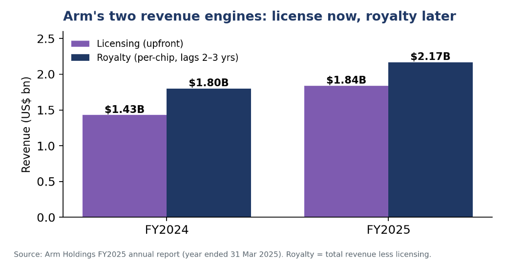
Arm’s IP model has a characteristic time lag that rewards patient analysis:
Because royalties lag licenses by two to three years, a surge in licensing today is an advance signal of royalty growth in 2027–28. Arm is also raising revenue per chip: its newer Armv9 architecture and pre-integrated Compute Subsystems (CSS) carry higher royalty rates than prior generations, and v9 already accounts for roughly a third of royalties. Annualized contract value (ACV) — a normalized measure of the licensing base — was growing around 28% year-on-year as of late 2025.
9. Demand drivers
Artificial intelligence — a double tailwind. AI raises demand in two ways. It multiplies the number and complexity of chips being designed (accelerators, networking, custom silicon), and it is being embedded inside the EDA tools themselves: ML-driven optimizers such as Synopsys’ DSO.ai and Cadence’s Cerebrus can close designs faster and better than manual methods, which the vendors sell as a high-margin premium.
Rising design complexity. Each new node (3nm, 2nm, gate-all-around) and each additional billion transistors increases verification and implementation effort, lifting tool consumption per design.
Chiplets, 3D-IC, and advanced packaging. Multi-die designs require new tools for partitioning, 3D floor-planning, thermal analysis, and die-to-die interconnect — a direct beneficiary of the same advanced-packaging wave reshaping the back-end, and a key motivation for the Synopsys-Ansys combination.
The custom-silicon boom. Hyperscalers designing their own chips (Google’s TPU, AWS’s Graviton and Trainium, Microsoft’s Maia, Meta’s MTIA) have multiplied the number of sophisticated design starts — each one a new consumer of EDA seats and licensed IP, often from customers who never previously designed silicon.
10. Geopolitics: design software as a chokepoint
EDA is a control point comparable to EUV lithography: the leading tools are supplied by two US companies and one US-based unit of a German firm, and they cannot be readily substituted. This was demonstrated vividly in 2025. On 23–29 May 2025, the US Bureau of Industry and Security imposed license requirements on EDA exports to China, abruptly cutting Chinese chip designers off from new tools, updates, and support. Barely six weeks later, on 2–3 July 2025, the restrictions were rescinded as part of a broader US-China framework that also eased China’s rare-earth export curbs.
The episode underscored several realities. China was a meaningful revenue source — roughly 16% of Synopsys and ~12% of Cadence revenue — so the controls hurt the vendors as well as their customers, and Siemens EDA reported a significant China revenue decline that quarter. It also accelerated China’s push for domestic EDA (Empyrean, Primarius, X-EPIC, and newer entrants such as Univista), though Chinese tools remain far behind on full-flow, leading-edge design. RISC-V adds a parallel dimension: as an open, license-free instruction set not owned by any single country’s company, it is attractive to Chinese designers seeking to reduce dependence on Arm.
Will US-headquartered EDA vendors see their total revenue share from the Asia-Pacific region (excluding Japan) drop below 20% in audited fiscal year 2026?
YesResult
0.00%
NoResult
100.00%
1 Polls
EndedTBD
11. A framework for financial analysis
• Value the recurring base and backlog. Time-based revenue mix, retention rates, and committed backlog (e.g., Synopsys’ $11.4 bn) are the core quality signals; they make revenue unusually predictable.
• For Arm, watch licensing as a leading indicator. Licensing and ACV today foreshadow royalties two to three years out; royalty-per-chip (the v9 and CSS mix) is the key margin lever.
• Track the AI attach rate. Adoption of AI-driven tools (DSO.ai, Cerebrus) is both a growth driver and a test of pricing power.
• Remember the sector is R&D-cycle, not capex-cycle. EDA/IP revenue is tied to customers’ design budgets, which are steadier than fab capital spending — a defensive quality versus the equipment names.
• Mind valuation. These are high-multiple equities; much of the value rests on durable growth and moats, so they are sensitive to any deceleration or to regulatory and geopolitical shocks.
PredictionMarkets Org disclaimer: This article is an educational overview, not investment advice, and does not constitute a recommendation to buy or sell any security.
12. Key debates to watch
• RISC-V versus Arm. Whether the open instruction set erodes Arm’s royalty economics in volume markets, or remains complementary at the edges.
• Arm moving up the stack. Arm’s shift toward pre-integrated subsystems (CSS) — and reports of its own chips — raises potential channel conflict with the customers it licenses to.
• AI in EDA: boon or pricing pressure? Whether AI tools mainly expand the premium tier, or eventually let customers do more with fewer seats.
• China’s domestic EDA. How quickly local vendors can close the gap on full-flow, leading-edge design — the sector’s equivalent of the EUV question.
• Concentration and antitrust. The Synopsys-Ansys deal required divestitures; further consolidation will draw scrutiny.
13. Risk summary
• Geopolitical/regulatory — export controls can cut off a ~10–16% revenue market overnight, as 2025 showed.
• Disruption risk — RISC-V (to Arm) and open-source EDA efforts (to the Big Three), though both remain early.
• Customer concentration and consolidation — a handful of large designers and foundries drive much of demand.
• Valuation/multiple risk — rich multiples leave little room for growth disappointment.
• Integration risk — absorbing Ansys is a large undertaking for Synopsys.
The capital-equipment and materials layer that enables all semiconductor's manufacturing — its structure, economics, leaders, and strategic risks.
Executive summary
The semiconductor equipment and semiconductor materials industry supplies the capital tools and consumable inputs required to manufacture every integrated circuit produced worldwide. It sits at the apex of the chip supply chain: its customers are the chip designers/fablesses, foundries, integrated device manufacturers (IDMs), and outsourced assembly-and-test houses (OSAT) that together constitute the rest of the industry. Because no advanced chip can be fabricated without these tools and materials, the sector functions as the binding constraint on global computing capacity — a position that confers both unusual pricing power and acute strategic sensitivity.
Three characteristics define the sector’s investment profile. First, structural concentration: a handful of firms control the majority of each process step, and several occupy de facto monopolies. 2) Second, deep and durable barriers to entry: leading-edge tools embody decades of accumulated process physics and are co-developed with customers years ahead of production, making displacement rare. Third, geopolitical centrality: because controlling the means of production is the most effective lever for controlling who can manufacture advanced chips, the sector has become the principal instrument of export-control policy between the United States, its allies, and China.
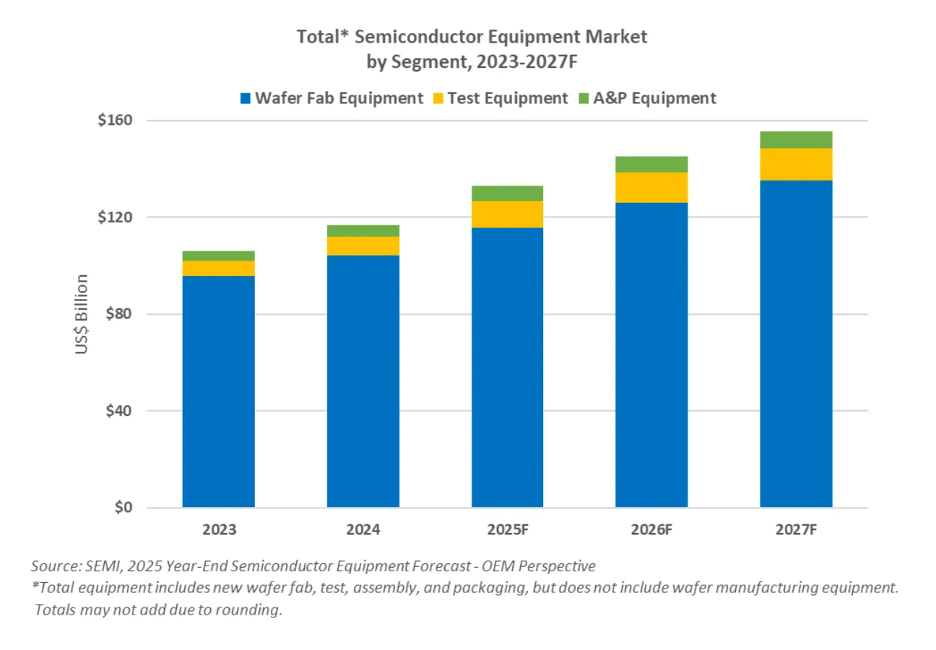
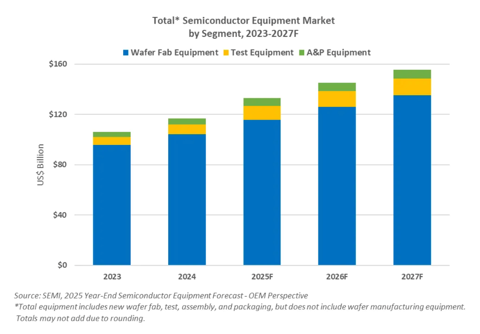
On the latest data, total semiconductor equipment sales reached a record $135 billion in 2025 and are forecast by SEMI to surpass $150 billion for the first time in 2027 (~$156 billion) (SEMI), while the separately-reported materials market set a record of $73.2 billion in 2025 (SEMI). The current cycle is distinguished less by unit volume than by complexity: artificial intelligence, high-bandwidth memory, and advanced packaging are reshaping where capital is deployed across the manufacturing flow.
1. Defining the sector and its strategic importance
For semiconductor equipments, a useful starting point is the economics of a modern fabrication plant (“fab”). A single leading-edge logic fab now requires a capital outlay on the order of $20–30 billion or more, of which the great majority — commonly 70–80% — is spent on process equipment rather than the building itself, based on our channel check and industry analysis. The equipment industry therefore captures the largest share of every wave of fab investment, and its revenues are a direct function of the capital-expenditure decisions of a small number of very large manufacturers (for example, TSMC, Samsung, Intel, and the memory producers).
The materials industry operates on a different rhythm. Where equipment is a periodic capital purchase, materials — silicon wafers, photoresist, process gases, substrates — are consumed continuously as long as a fab is running. This gives the materials business steadier, utilization-linked revenue that is far less volatile than equipment demand, an important distinction for portfolio construction.
Taken together, the sector is best understood not as a supplier of components but as the owner of the enabling technology for the entire digital economy. Its products are the precondition for every downstream activity, which is why a relatively modest revenue base (roughly $200 billion across equipment and materials combined in 2025, according to SEMI) commands disproportionate strategic and financial attention.
2. Position in the value chain
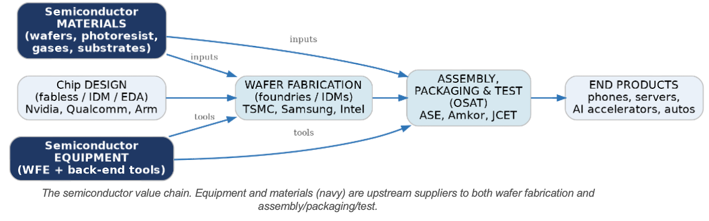
The chip moves through a sequential value chain, with equipment and materials feeding in from upstream. Crucially, equipments & materials supply both ends of manufacturing — the front-end fabs that build circuits on the wafer, and the back-end houses that package and test finished devices. The equipment vendor is always upstream of whoever operates the tool.
This distinction resolves a common point of confusion. “Assembly, packaging, and test” denotes both a service (performed downstream by OSAT firms such as ASE and Amkor) and the equipment used to perform it (supplied upstream by tool vendors). The back-end equipment is upstream of back-end manufacturing; the naming overlaps, but the economic roles do not.
3. How chips are made — and where each tool fits
Understanding the sector requires understanding the manufacturing flow, because each major equipment category maps to a specific process step. Fabrication divides into a front-end phase (building the transistors and interconnect on the wafer) and a back-end phase (singulating, packaging, and testing the finished chips).
Front-end: a repeated build-up of layers
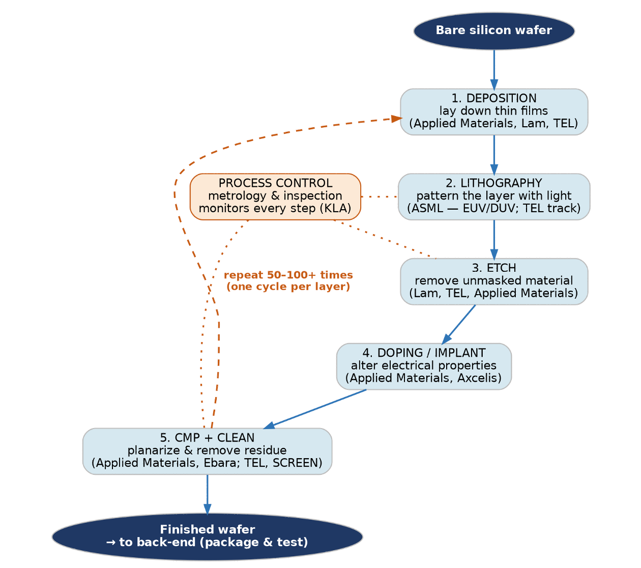
The front-end does not run once; it is a cyclical process repeated 50 to more than 100 times, once for each layer of the device. A simplified cycle proceeds as follows:
Each pass deposits material, patterns it with light, and etches away what is not needed, with doping, planarization, and cleaning interspersed. Because the cycle repeats so many times, even small per-step improvements in yield or throughput compound enormously — which is why customers are reluctant to switch qualified tools and why incumbents enjoy such durable positions. As devices migrate to advanced architectures (FinFET and now gate-all-around transistors, plus 3D memory stacking), the number of deposition and etch steps has risen sharply, increasing the equipment intensity of each wafer and benefiting the deposition/etch leaders in particular.
Back-end: from wafer to packaged, tested chip
Once the wafer is complete, the back-end dices it into individual dies, attaches and connects them within a package, and tests the result. Historically a lower-value, slower-growing segment, the back-end has been transformed by advanced packaging, which increasingly uses wafer-level, fab-style processes and so blurs the traditional front-end/back-end boundary.
4. Market size and segmentation
We summarize semiconductor equipment and materials in two separate SEMI data sets. The equipment figures come from SEMI’s Year-End Total Semiconductor Equipment Forecast; the materials figures come from SEMI’s annual Materials Market report. The two markets differ in size, segmentation, and cyclicality, so combining them obscures more than it reveals.
4.1 The equipment market
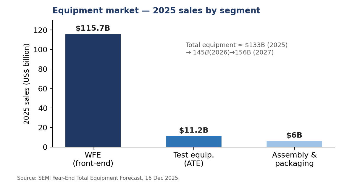
Per SEMI’s Year-End Total Equipment Forecast (16 December 2025), total semiconductor manufacturing equipment sales reached a record $133 billion in 2025 (+13.7% year-on-year), and are projected to grow to $145 billion in 2026 and $156 billion in 2027 — surpassing $150 billion for the first time. Wafer fab equipment (WFE) dominates, while the back-end (test and packaging) has rebounded sharply off a smaller base.
Equipment
segment
2025 sales
2025 growth
Trajectory
to 2027
WFE (front-end)
$115.7 bn
+11.0% (from $104 bn in
2024)
→ $135.2 bn by 2027
(advanced logic, DRAM/HBM)
Test equipment (ATE)
$11.2 bn
+48.1%
+12.0% 2026, +7.1% 2027 (AI/HBM test complexity)
Assembly & packaging
$6.0 bn
+19.6%
+9.2% 2026, +6.9% 2027
(advanced packaging)
Total equipment
$133 bn
+13.7%
→ $145 bn 2026 → $156 bn 2027
Within WFE, foundry-and-logic applications alone accounted for roughly $66.6 billion in 2025 (+9.8%), reflecting resilient leading-edge spending. China, Taiwan, and Korea are expected to remain the top three equipment-buying regions through 2027.
4.2 The materials market
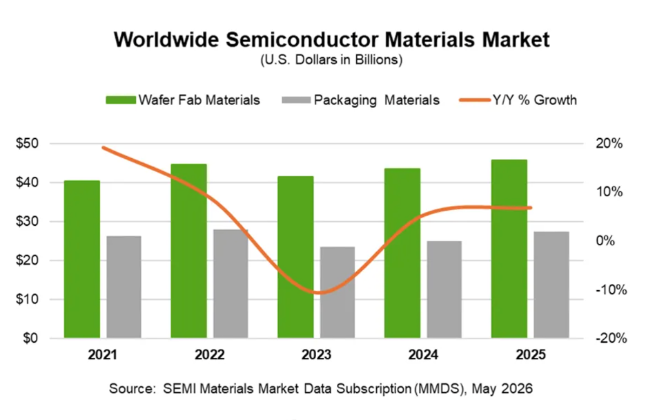
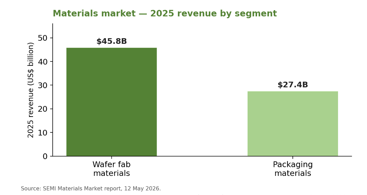
Per SEMI’s Materials Market report (12 May 2026) — a wholly separate release — global semiconductor materials revenue reached a record $73.2 billion in 2025 (+6.8% year-on-year). Materials are consumables purchased continuously as fabs run, so this market is steadier and less cyclical than equipment. It divides into wafer fab materials (used in front-end fabrication) and packaging materials (used in back-end assembly).
Substrates, bonding wire, lead frames, encapsulants
Total materials
$73.2 bn
+6.8%
—
Geographically, the materials data show where chips are actually built. Taiwan was the largest consumer for the 16th consecutive year (~$21.7 billion in 2025), followed by China (~$15.6 billion) and South Korea (~$11.2 billion). A related SEMI release (Feb 2026) noted that silicon wafer shipments rose 5.8% in 2025 to a record area, even as wafer revenue dipped slightly — a sign that AI-driven demand is concentrated in higher-value advanced wafers.
Top
materials consumers (2025)
Revenue
Taiwan (16th consecutive
year as #1)
~$21.7 bn
China
~$15.6 bn
South Korea
~$11.2 bn
5. Equipment segments and their leaders
The front-end equipment market is segmented by process step, with a clear leader (often a near-monopolist) in each:
· Lithography — the highest-value and most concentrated step, patterning circuits onto the wafer with light. ASML is the sole producer of extreme-ultraviolet (EUV) systems, which use 13.5-nanometer light to print the smallest features; its next-generation High-NA EUV tools cost in excess of $350 million each. ASML also leads advanced deep-ultraviolet (DUV) immersion lithography, with Canon and Nikon present at older nodes.
· Deposition — building up thin films via CVD, PVD, ALD, and epitaxy. Led by Applied Materials, Lam Research, and Tokyo Electron (TEL). Atomic-layer deposition in particular has grown with gate-all-around transistors and 3D memory.
· Etch — selectively removing material. Lam Research and Tokyo Electron lead, with Applied Materials present; high-aspect-ratio etch for 3D NAND and advanced logic is a key battleground.
· Process control (metrology & inspection) — measuring dimensions and detecting defects to protect yield. KLA holds a commanding position, and its importance rises as devices grow more complex; this segment also carries the highest margins in the industry.
· Other front-end steps — cleaning and surface preparation (TEL, SCREEN), ion implantation (Applied Materials, Axcelis), chemical-mechanical planarization (Applied Materials, Ebara), and thermal processing. Notably, TEL holds an estimated 88–90% share of the coater/developer (“track”) tools that pair with lithography.
Back-end equipment is more fragmented but faster-growing:
· Assembly & packaging tools — wire, die, flip-chip, and hybrid bonders; leaders include ASMPT, Kulicke & Soffa, and Besi. Hybrid bonding is the critical enabler of 3D stacking.
· Test equipment (ATE) — a duopoly of Teradyne and Advantest; Advantest in particular has benefited from the surge in testing intensity for AI accelerators and HBM.
6. Materials segments and their leaders
Materials feature their own deep moats: a contaminant measured in parts-per-billion can destroy a wafer, qualification cycles run for years, and switching costs are high.
• Silicon wafers — the substrate, led by Shin-Etsu and SUMCO of Japan, with GlobalWafers and Siltronic also major. Worldwide wafer shipments rebounded in 2025–26 on AI demand (SEMI).
• Photoresist and ancillaries — light-sensitive chemicals central to lithography. Japanese suppliers — Tokyo Ohka Kogyo (TOK), JSR, and Shin-Etsu — together hold more than half the global market, with leadership in EUV and ArF-immersion resists. This is among the most R&D-intensive material categories.
• Specialty gases and wet chemicals — Air Liquide, Linde, Merck, and others; consumption rises with process-step count.
• Photomasks, CMP slurries/pads, and sputtering targets — specialized consumables across the front-end flow.
• Packaging materials — substrates (notably ABF substrate), bonding wire (cost tied to gold prices), lead frames, and encapsulants. The fastest-growing materials sub-segment, driven by advanced packaging and the higher material intensity of multi-die AI chips; packaging materials grew 9.3% to $27.4 billion in 2025 (SEMI).
7. Competitive structure and company financials
The sector’s defining commercial feature is oligopoly with monopoly pockets. The five largest equipment suppliers — Applied Materials, ASML, Tokyo Electron, Lam Research, and KLA — together command an estimated 56–66% of the equipment market, and the leader in each individual step typically holds a far higher share still.
The financial signature of this structure is high and persistent margins, substantial recurring service revenue, strong returns on equity, and large capital returns. The latest full-year results illustrate the point:
Company
Core
franchise
FY2025
revenue
Gross margin
Net income
ASML
Lithography (sole EUV maker)
€32.7 bn (~$35 bn)
52.8%
€9.6 bn
Applied Materials
Broadest front-end + services
$28.4 bn
48.7%
~$7.0 bn
Lam Research
Etch & deposition +
services
$18.4 bn
48.7%
$5.36 bn
KLA
Process control / inspection
$12.2 bn
~60.9%
$4.06 bn
Several financial themes emerge from these disclosures:
• Margin hierarchy reflects competitive intensity. KLA’s ~61% gross margin — well above the ~49–53% of the others — reflects its dominant, lightly-contested position in process control. ASML’s margins are buoyed by the EUV monopoly.
• Recurring service revenue is a stabilizer. Service (spares, upgrades, field options on the installed base) is roughly 23% of revenue at ASML, Applied Materials, and KLA, and a notably higher ~43% at Lam Research — a meaningful cushion against the equipment cycle.
• Returns and capital allocation are aggressive. All five majors generate returns on equity above 30%. ASML authorized a new buyback of up to €12 billion (through 2028); Applied Materials repurchased ~$4.9 billion of stock in fiscal 2025. These are cash-generative, capital-light franchises.
• Customer and geographic concentration is high. Applied Materials’ two largest customers represented roughly 19% and 15% of revenue in FY2025; Lam Research derived 34% of fiscal-2025 revenue from China. Concentration is both a source of scale economics and a risk.
Tokyo Electron, the largest Japanese supplier and the third/fourth-largest globally, rounds out the front-end “big five” with its track dominance and strong etch/deposition franchises; precise figures follow its own (April-ending) fiscal calendar.
8. Demand drivers: an AI- and complexity-led cycle
The present up-cycle is driven by architecture and complexity rather than unit volume. The principal drivers:
Artificial intelligence and high-performance computing. Training and serving large models requires vast quantities of leading-edge logic and high-bandwidth memory (HBM), pulling WFE for advanced nodes and for DRAM/HBM capacity. KLA’s management has explicitly tied its return to leading-edge growth to “expanding AI and high-performance computing investments.”
The end of easy transistor scaling and the rise of advanced packaging. As shrinking transistors becomes harder and costlier, performance increasingly comes from packaging — stacking and interconnecting multiple dies and memory. The advanced-packaging market was roughly $33–38 billion in 2024–25, growing at a double-digit CAGR, and by some estimates surpassed traditional packaging as a majority of total packaging value in 2025 (Yole). TSMC’s CoWoS platform is the marquee example: CoWoS wafer demand is forecast to rise roughly 40% year-over-year into 2026, driven overwhelmingly by Nvidia.
Memory as a strategic asset. HBM has converted DRAM from a boom-bust commodity into a constrained, high-value product, prompting elevated memory-equipment spending. This is the proximate cause of the upward revisions to WFE forecasts through 2027.
Because advanced packaging increasingly relies on wafer-level processes, front-end-style tools (deposition, etch, lithography) are migrating into the back-end, expanding the addressable market for the large front-end vendors and partly explaining their strategic push into packaging.
9. The dominant risk: geopolitics and export controls
Export controls now move the sector’s share prices. The governing logic is that controlling the tools is more effective than controlling the chips: a lithography system is a ~$200 million asset requiring years of vendor servicing, whereas a finished chip is a commodity that can be rerouted. The United States and its allies (the Netherlands and Japan, home to ASML, TEL, Nikon, Canon, SCREEN, and Advantest) have progressively restricted exports of advanced equipment to China.
The state of play as of mid-2026:
• EUV is fully denied to China. ASML’s EUV tools have never been sold there; no domestic alternative exists, and China’s SMEE remains far behind on indigenous lithography.
• DUV and servicing are the live battleground. SMIC and Hua Hong still use ASML’s DUV immersion tools, applying multipatterning to reach 7nm-class chips. Proposed US legislation (the MATCH Act) would tighten DUV and etch controls and press allies to align.
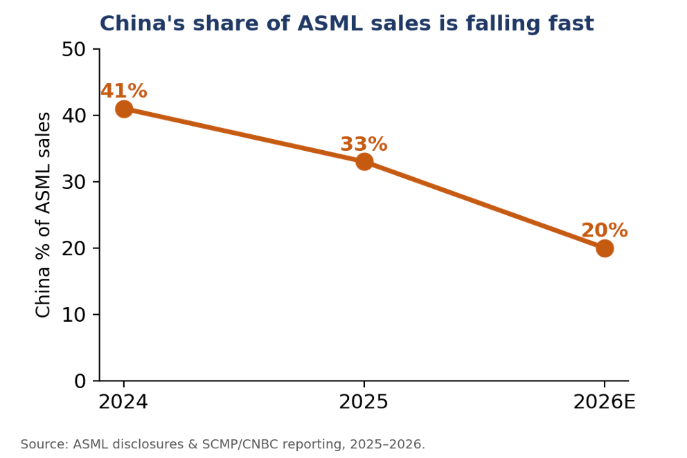
• Western vendors’ China exposure is falling sharply. China’s share of ASML sales declined from roughly 41% (2024) to 33% (2025), with guidance toward ~20% in 2026.
• China is accelerating self-sufficiency. Beijing has reportedly mandated at least 50% domestic equipment sourcing, with a 15th Five-Year-Plan target of ~80% self-sufficiency by 2030, a fully domestic 7nm equipment line, and stable 14nm production. Domestic suppliers (NAURA, AMEC, and SiCarrier-linked entities) are gaining share in mature-node and packaging tools.
The widely noted irony is that aggressive controls are accelerating China’s domestic investment, pushing the world toward two parallel supply chains. For investors this is double-edged: a near-term loss of a large market for Western vendors, and the longer-term emergence of subsidized domestic competitors at the low-to-mid end.
10. A framework for financial analysis
Several principles help in evaluating companies in the sector:
• Track the capex cycle through leading indicators. Equipment demand follows customer capital budgets; monitor the capex guidance of TSMC, Samsung, Intel, and the memory makers, plus fab-utilization rates and company backlog and bookings (ASML’s quarterly net bookings, which reached €13.2 billion in Q4 2025, are a closely watched signal).
• Use “WFE intensity” as a structural lens. Because each node transition adds deposition, etch, and patterning steps, WFE spending per wafer tends to rise structurally even when wafer volumes are flat — a secular tailwind beneath the cycle.
• Value the recurring base. Service and installed-base revenue is higher-margin and far steadier than tool sales; a larger service mix (e.g., Lam’s ~43%) warrants a more defensive valuation.
• Watch margin persistence and R&D intensity. Sustained high gross margins signal pricing power; sustained heavy R&D (ASML alone spent €4.7 billion in 2025) is the price of staying ahead — falling R&D is a warning, not a saving.
• Pair equipment with materials. Equipment offers torque to the capex cycle and the highest margins; materials offer steadier, utilization-linked revenue. Holding both balances cyclicality.
This document is an educational overview, not investment advice, and does not constitute a recommendation to buy or sell any security.
11. Key debates to watch
• Durability of the AI capex cycle — multi-year structural build-out versus eventual digestion and over-build.
• Who captures advanced packaging — foundries (TSMC), OSATs (ASE, Amkor), and equipment makers are all advancing; the economics of process and tool ownership are still being decided.
• Pace of China’s indigenization — mature nodes and packaging appear achievable; EUV and the most advanced steps remain a steep, multi-year climb.
• HBM/memory cyclicality — whether HBM stays supply-constrained or swings back to a glut is a key swing factor for memory-exposed equipment demand.
12. Risk summary
• Cyclicality in fab capital expenditure, amplified for the most equipment-levered names.
• Customer concentration — a few foundries and memory makers drive a large share of demand.
• Geopolitical and regulatory risk — export controls can remove a large market quickly and are subject to political change.
• Technology-transition risk — a missed node or packaging transition can permanently shift share.
• Long qualification cycles in materials can delay new-product revenue.
Will ASML's full-year 2026 net sales beat €40 billion (guided in April 2026?
YesResult
75.00%
NoResult
25.00%
4 Polls
Ended
Which company will see the biggest gross margin increase for its fiscal year vs prior fiscal year?